


Industrial Solutions
Industrial IoT Gateway vs. Edge Computing Gateway: A 2026 Comparison
At a Glance
- The convergence of operational technology (OT) and information technology (IT) has created urgent demand for devices that can bridge the physical world with cloud-native data platforms – at the edge, in real time, and with carrier-grade reliability.
- Industrial IoT gateway deployments are accelerating as manufacturers, utilities, and transportation operators seek to extract intelligence from previously isolated machinery and field sensors.
- IIoT edge computing adds a new dimension to this challenge: processing data locally before it ever reaches the cloud, reducing latency, saving bandwidth, and enabling real-time autonomous decisions.
- Understanding the difference between an industrial IoT gateway and a true edge computing gateway – and knowing which vendors deliver both in a single, purpose-built platform – is now a strategic imperative for industrial operators.
Factory floors, substations, oil pipelines, and smart highways all share a common challenge: they generate enormous volumes of operational data from sensors, PLCs, and SCADA systems, but they lack the network intelligence to make that data instantly actionable. The industrial IoT gateway has emerged as the critical device that solves this problem – and as iiot edge computing matures, the most capable gateways are now doing far more than simple data aggregation.
Defining the Industrial IoT Gateway
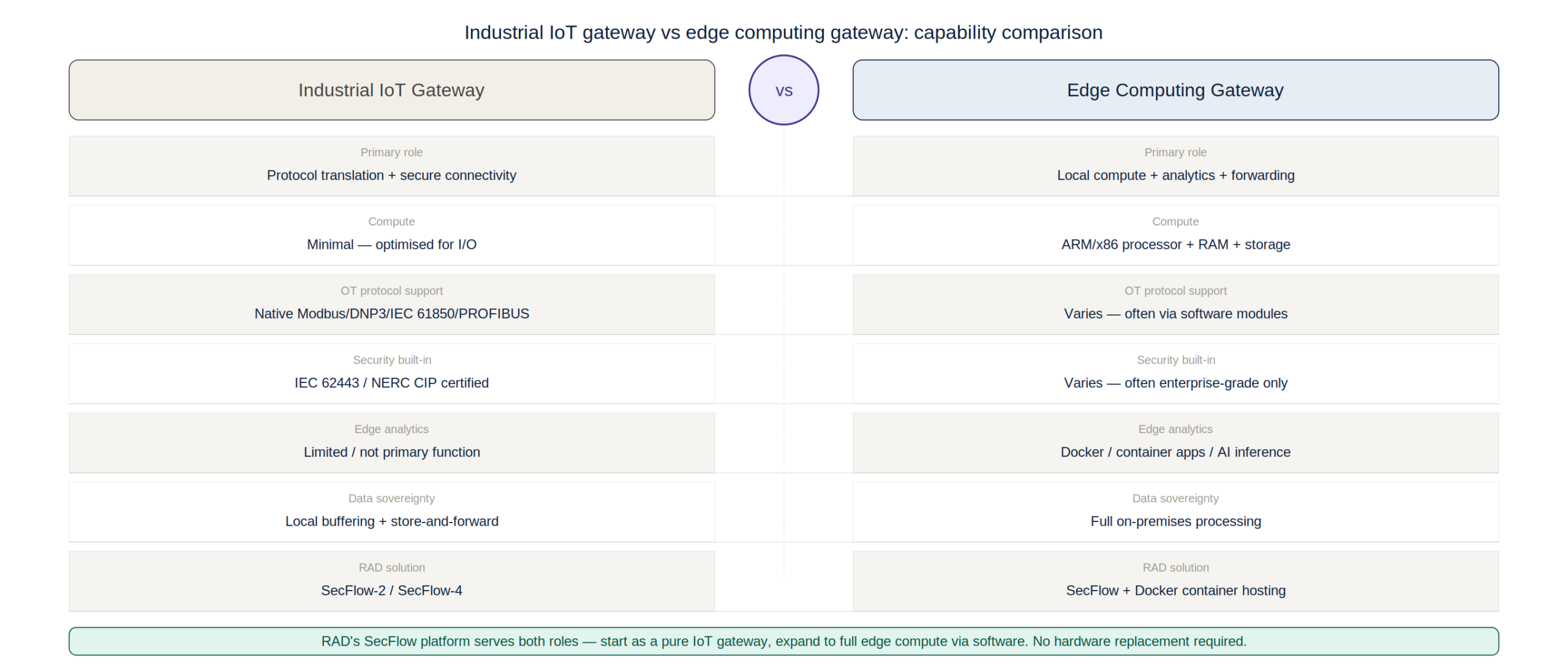
An industrial IoT gateway is a rugged, purpose-built device designed to collect data from industrial sensors, machines, and legacy protocols (Modbus, DNP3, IEC 61850, PROFIBUS) and convert it into IP-based data streams that cloud platforms and enterprise systems can consume. Unlike consumer IoT devices, IIoT gateways must operate in extreme temperatures, withstand vibration and electromagnetic interference, and maintain connectivity even during network disruptions.
The core functions of an industrial IoT gateway include protocol translation, data normalization, secure connectivity (VPN, TLS, certificate management), local buffering for store-and-forward resilience, and remote management over out-of-band channels. These are non-negotiable capabilities for any operator managing critical infrastructure.
Leading IIoT gateways also support zero-touch provisioning, enabling large-scale deployments of hundreds or thousands of devices without requiring on-site engineering expertise at each location – a feature that dramatically reduces the total cost of large industrial connectivity projects.
What Makes an Edge Computing Gateway Different?
An edge computing gateway goes beyond aggregation and forwarding. It embeds compute resources – typically an ARM or x86 processor with sufficient RAM and storage – that allow local execution of analytics workloads, machine learning inference models, and business logic. Rather than shipping raw sensor data to a distant cloud server for analysis, an edge computing gateway processes it locally and sends only actionable results or compressed summaries upstream.
This distinction matters enormously in industrial environments where network bandwidth is constrained, latency requirements are sub-100ms, or where cloud connectivity is intermittent. A smart city traffic controller, a substation protection relay, or an autonomous mobile robot cannot wait 500ms for a cloud round-trip before making a safety-critical decision.
IIoT edge computing platforms also enable local data sovereignty – keeping sensitive operational data on-premises while still feeding aggregated, anonymized insights to enterprise dashboards. For regulated industries including utilities, healthcare, and defense, this is not a nice-to-have but a compliance requirement.
Comparing the Leading Vendors in 2026
The IIoT gateways market in 2026 is served by a range of vendors with very different strengths. Advantech’s WISE series offers strong edge compute capability with a broad software ecosystem but can be challenging to deploy in harsh outdoor environments without additional enclosures. Moxa’s EDR and MGate lines excel at serial-to-IP protocol conversion but have more limited native edge analytics capabilities. Cisco’s IR1100 series targets enterprise-grade security but comes with significant cost and complexity overhead.
RAD Data Communications takes a different approach with its SecFlow family and multiservice access gateways. Rather than positioning its devices as either pure IoT gateways or pure compute platforms, RAD delivers integrated platforms that combine rugged industrial connectivity with carrier-grade networking features and optional edge intelligence – all managed through a unified, open management framework.
This integration matters because industrial operators increasingly need their edge devices to handle multiple roles: connecting legacy OT assets, enforcing cybersecurity policies, providing cellular failover, and running lightweight analytics – ideally all within a single managed device rather than a stack of separate appliances.
RAD’s Approach to Industrial IoT and Edge Computing
RAD’s SecFlow-2 and SecFlow-4 gateways represent a mature answer to the industrial IoT gateway challenge. Designed for mission-critical environments including substations, water treatment plants, rail networks, and smart city deployments, they combine IEEE 802.1X network access control, deep packet inspection, and industrial protocol support (IEC 61850, DNP3, Modbus TCP) within a hardened, DIN-rail-mountable platform.
For iiot edge computing requirements, RAD’s platform supports Docker container hosting, enabling operators to deploy purpose-built analytics applications alongside connectivity functions without additional hardware. This containerized approach allows software updates without device replacement, dramatically extending hardware lifecycle and reducing capital expenditure cycles.
RAD’s unified management through its Service Assured Access framework provides centralized visibility into device health, connectivity status, security events, and application performance – from a single pane of glass that integrates with leading OSS/BSS platforms via open APIs. This is the operational model that modern industrial operators require.
Security: The Non-Negotiable Differentiator
In industrial environments, cybersecurity is not a feature – it is a prerequisite. Industrial IoT gateways and edge computing gateways that lack robust, built-in security are not just insufficient; they are actively dangerous. A single compromised gateway in a power substation, a water treatment plant, or a transportation network can have catastrophic physical consequences.
RAD’s SecFlow platforms embed enterprise-grade security by design: stateful firewall, IDS/IPS, VPN termination, certificate-based authentication, and automated anomaly detection. They are compliant with IEC 62443 industrial cybersecurity standards and NERC CIP requirements for critical infrastructure protection – standards that many competing IIoT gateways simply do not address at the hardware level.
The ability to enforce micro-segmentation between OT zones – isolating PLCs from SCADA servers, and both from enterprise IT networks – is a specific SecFlow capability that goes well beyond what typical edge compute platforms provide.
Choosing the Right Platform for Your Industrial Network
The choice between a dedicated industrial IoT gateway and a full edge computing gateway increasingly depends on the maturity of your operational analytics program. If your primary need is reliable OT connectivity, protocol conversion, and secure remote management, a purpose-built IIoT gateway with strong networking credentials is the right foundation. If you are already running or planning to deploy real-time analytics, AI inference, or autonomous control logic at the edge, a platform with embedded compute and an open application runtime is essential.
RAD’s portfolio is designed to support both needs – and to grow with your requirements. Devices can be deployed initially as pure connectivity gateways and upgraded to full edge compute platforms via software, preserving capital investment while enabling operational evolution.
For industrial operators seeking a vendor with deep domain expertise, proven deployments across utilities, transportation, and manufacturing, and a commitment to open standards and long-term product support, RAD represents the benchmark against which industrial IoT gateway and edge computing gateway solutions should be evaluated.

Industrial Solutions
Industrial IoT Gateways for Remote Asset Monitoring: What Utilities and Infrastructure Operators Need to Know
Deploying industrial IoT gateways for remote asset monitoring allows critical infrastructure firms to manage distributed field assets that stretch across thousands of kilometers safely. Whether the assets are power transmission towers, water pump stations, or unattended substations, operators face a shared problem. They need real-time visibility into equipment that is physically far away and exposed to harsh weather elements. Furthermore, these networks must operate over unreliable or highly constrained communication links.
These specialized gateways sit at the field edge to aggregate data from remote sensors and control equipment. Consequently, they process data locally where needed and relay it securely to centralized management platforms. Selecting the right gateway platform remains a critical decision. The wrong choice creates connectivity gaps, cybersecurity exposure, and an intense maintenance burden that erodes structural efficiency gains.
Operational Challenges Mitigated by Edge Infrastructure
Transitioning from legacy manual diagnostics to automated field nodes resolves multiple systemic bottlenecks for modern utility teams. For example, a failure to monitor transformer health results in massive network outages.
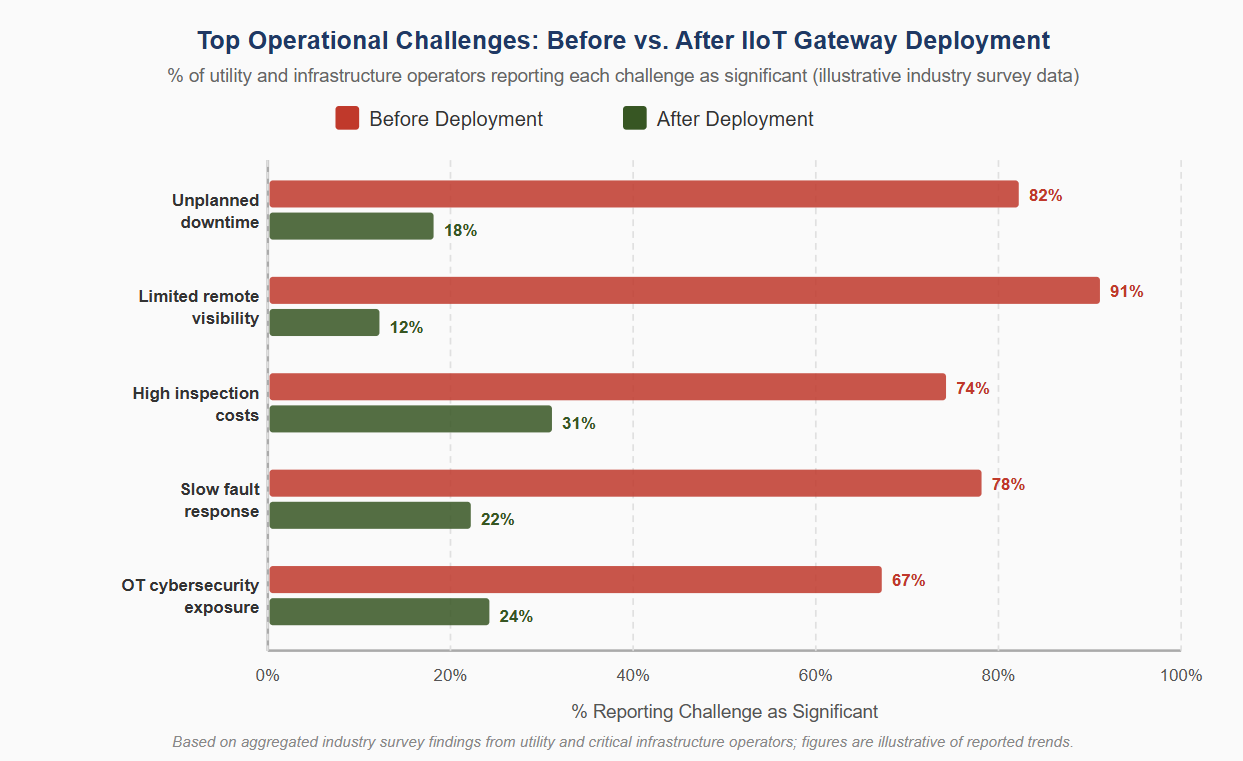
The chart below shows the top operational challenges reported by utility and infrastructure operators before and after deployment campaigns:
| Requirement | Power Utilities | Water & Wastewater | Oil & Gas | Transportation |
| Legacy Protocols | IEC 61850, DNP3 | Modbus, DNP3 | Modbus, PROFIBUS |
IEC 61375, Modbus |
| Operating Temp | -40°C to +70°C | -20°C to +60°C | -40°C to +70°C |
-40°C to +70°C |
| Comms Redundancy | Fiber + LTE failover | LTE primary / backup | Satellite + LTE |
LTE + Wi-Fi backup |
| Cybersecurity Standards | IEC 62443, NERC CIP | NIST CSF | IEC 62443 |
NIS2, IEC 62443 |
| Certifications | IEC 61850-3, IEEE 1613 | IP67, ATEX (some) | ATEX, IECEx |
EN 50121-4 |
Core Tasks of Hardware at the Network Edge
It is worth being precise about what distinguishes an industrial gateway from a generic office router or a basic consumer hub. Field sensor networks use old serial protocols like Modbus RTU or DNP3. Therefore, the gateway handles protocol conversion by translating these legacy formats into modern IP-based data streams.
In addition, embedding edge compute capabilities within the hardware layer allows for rapid data compression and local threshold detection. This localized processing keeps bandwidth consumption minimal. Furthermore, field components feature extensive environmental hardening. This enables them to survive wide temperature fluctuations between -40°C and +70°C without mechanical failure.
Managing Connectivity and Private Cellular Channels
Field site connectivity architectures vary based on geography. While some central facilities utilize fiber lines, distant installations rely completely on public cellular or satellite communication links. As a result, gateways require automated link switchover capabilities and dual SIM slot structures to maintain data integrity.
Furthermore, utilities are increasingly deploying private LTE and private 5G campus networks to gain dedicated wireless coverage. Modern hardware choices must support these private bands alongside standard WAN interfaces to eliminate coverage gaps. To optimize asset health over long distances, operators frequently combine these channels with specialized power line monitoring solutions to protect linear infrastructure lines.
Hardening Operational Technology Cybersecurity Postures
Operational technology (OT) environments were historically air-gapped from corporate networks. However, that physical isolation no longer exists in modern utility architecture. Every connected edge device introduces a potential attack surface that malicious actors can target.
Consequently, procurement teams must enforce strict compliance with international security frameworks. For example, the IEC 62443 standard dictates device authentication, role-based access control, and encrypted data transmission paths. Operators must verify these compliance logs independently to protect decentralized networks against unauthorized systemic access.
Shortlist Criteria for System Fleet Evaluation
When choosing an edge gateway platform, engineering directors should look for native protocol breadth rather than relying on generic vendor claims. In addition, require official test certificates for sector-specific hazards like ATEX zones or railway vibrations. Fleet management is also critical. Because managing hundreds of individual locations manually is impossible, platforms must offer zero-touch provisioning and secure over-the-air (OTA) firmware updates. Finally, confirm that the vendor guarantees long-term hardware availability and patch support across a standard fifteen-year asset lifecycle.
Conclusion
Remote diagnostics have transitioned from a premium best-practice to a baseline requirement across critical infrastructure networks. The field gateway provides the foundational intelligence that makes this scaling viable. However, this success is only possible when the hardware matches the strict realities of the deployment zone. Taking shortcuts in the selection phase creates expensive field failures within the first year of deployment. In contrast, selecting a secure, hardened substation automation gateway ensures that grid monitoring remains continuous, resilient, and safe over decades of service.
Review Disclaimer
This independent technical analysis is intended for industrial evaluation and network planning purposes only. Operational metric reductions, protocol conversion speeds, and link failover times vary based on local RF conditions, firmware configurations, and backend management setups. Critical infrastructure operators must independently verify hardware test certificates and run closed-loop pilot tests before executing large-scale edge deployments.
Greenhouse Specialty Tomatoes: Optimizing Brix and Flavor Profiles
The commercial cultivation of vine-ripened produce within controlled environment agriculture (CEA) spaces has shifted from basic volume tracking to strict quality and flavor management. For greenhouse agronomists, major estate developers, and premium grocery suppliers, producing a high-yield fresh tomato harvest requires balancing water inputs, lighting schedules, and specialized plant nutrition. Historically, large-scale tomato production prioritized total fruit weight and transport firmness over consumer taste profiles. This focus often resulted in watery, low-sugar tomatoes that failed to secure premium pricing from modern retail networks or gourmet food distributors.
To capture high-margin retail positions, progressive greenhouse operations are utilizing advanced agronomic selection models to maximize natural sugar concentrations and flavor depth. Shifting focus toward sweetness metrics and balanced acidity levels enables growers to deliver intense, uniform flavor profiles that command premium shelf space. This technical analysis breaks down the chemical factors that drive fruit flavor, evaluates the resource efficiency of advanced greenhouse systems, and demonstrates how specialized seed genetics secure consistent quality in large-scale operations.
The Chemistry of Taste: Managing Brix Concentration
The commercial value of specialty snacking produce is heavily dictated by its rating on the Brix scale, which measures the percentage of dissolved solids—primarily natural sugars—within the fruit’s juice. Standard commodity tomatoes frequently display low Brix scores, resulting in a bland taste profile that alienates premium consumer groups. Achieving a superior flavor profile requires seed varieties that naturally channel nutrients into sugar development without compromising vine vigor or fruit skin strength.
Utilizing dedicated genetic platforms to select tomato breeders and high-brix strains solves these quality variations completely. Advanced agronomic systems manage greenhouse microclimates and root nutrition to support the natural strengths of specialized seed lines. This targeted approach enables growers to produce a snacking tomato that consistently achieves excellent sugar concentrations, ensuring every harvest matches strict retail flavor profiles.
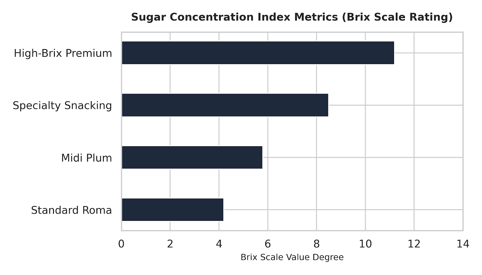
Quantitative Comparison: Sugar Concentrations on the Brix Scale
Field data from greenhouse operations confirms that seed genetics are the primary factor dictating final fruit sweetness. While climate controls optimize plant health, specialized crop varieties are essential to reach top-tier sugar concentrations.
The chart below outlines the average sugar concentration scores achieved across different tomato classifications under standardized controlled greenhouse conditions:
📈 Sugar Concentration Index Metrics (Brix Scale Rating)
Securing Visual and Textural Uniformity in Specialty Produce
Maximizing fruit sweetness provides limited value if the harvest lacks structural uniformity. Retail distribution buyers demand absolute consistency in shape, weight, and color across every shipment to match automated grocery displays, such as specialized greenhouse tomato varieties and premium plum tomato varieties.
A thorough review of premium supply networks shows that integrating advanced specialty tomatoes lines and high-yield tomato umami varieties secures long-term market access. These varieties develop thick cell walls that resist cracking during transport while packing intense natural flavor. By aligning greenhouse production with advanced flavor genetics, commercial operators protect their crops from bruising and establish reliable, premium revenue streams throughout the year.
Conclusion
Relying on low-brix commodity crop lines within high-cost controlled environment agriculture spaces limits revenue potential and increases vulnerability to market price swings. Shifting production over to high-brix specialty tomato varieties provides greenhouse operators and grocery suppliers with a reliable way to maximize fruit quality, secure premium market pricing, and build strong consumer brand loyalty. As retail quality audits and distributor selection criteria continue to tighten, deploying advanced flavor-driven crop genetics remains a fundamental strategy for scaling profitable greenhouse infrastructure.
At a Glance
- Aerial survey is undergoing its most significant transformation in decades – driven by higher-resolution sensor technology, AI-accelerated processing, and the growing demand for sub-centimetre accuracy across infrastructure, urban planning, and environmental monitoring.
- Aerial mapping software has evolved from post-processing pipelines into real-time integrated platforms that manage sensor data, flight planning, georeferencing, and deliverable production in a single workflow.
- The choice of sensor and software defines the accuracy, efficiency, and commercial viability of every aerial survey project – making platform selection a strategic decision, not just a procurement one.
- Phase One’s integrated approach — combining the world’s highest-resolution aerial cameras with the iX Suite software platform – sets the benchmark against which all aerial survey and mapping solutions should be evaluated.
There has never been more demand for accurate, high-resolution aerial survey data — and never more choice in how to acquire it. Government agencies mapping national infrastructure, urban planners building 3D city models, environmental scientists monitoring deforestation, and engineering firms conducting corridor surveys all depend on aerial survey capability that delivers reliable, precise, and rapidly processed geospatial intelligence. The sensor and aerial mapping software combination chosen for these missions determines whether they succeed.
The Aerial Survey Technology Landscape in 2026
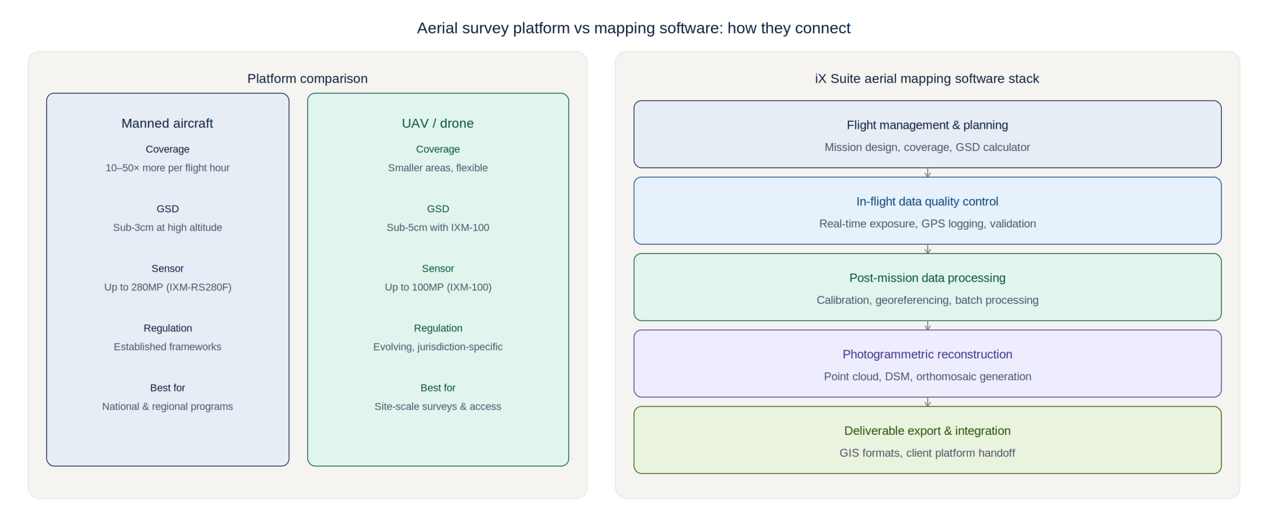
Aerial survey is no longer the exclusive domain of manned fixed-wing aircraft carrying large-format film cameras. The market today spans a continuum from consumer-grade drone photogrammetry at one end to precision manned aircraft systems carrying 280-megapixel digital sensors at the other – with a corresponding range of accuracy specifications, operational complexity, and project economics.
At the high-precision end of the spectrum, large-format digital aerial cameras mounted on fixed-wing aircraft remain the gold standard for national mapping programs, large-area infrastructure surveys, and applications requiring sub-5cm ground sample distance over extensive coverage areas. Phase One’s IXM camera family – including the IXM-100 (100MP) and IXM-RS280F (280MP) – represent the current state of the art in this category, delivering the combination of sensor size, dynamic range, and geometric stability that large-scale aerial survey demands.
At the mid-market level, UAV-based survey systems using high-quality imaging sensors have dramatically reduced the cost of aerial survey for projects where coverage areas are measured in hundreds rather than thousands of square kilometres. Phase One’s UAV camera solutions bridge this segment, offering the sensor quality of professional mapping cameras in form factors compatible with industrial drone platforms.
Aerial Survey: Manned Aircraft vs UAV Platforms
The choice between manned aircraft and UAV platforms for aerial survey involves five key trade-offs. First, coverage efficiency: manned platforms at cruising altitude cover 10-50× more ground per flight hour than multi-rotor UAVs, making them the only viable option for national or regional mapping programs. Second, accuracy: both platforms can achieve centimetre-level accuracy with RTK/PPK positioning and precision sensors, but manned platforms with forward motion compensation and gyro-stabilised mounts produce superior results across variable terrain.
Third, regulatory complexity: manned aerial survey operates under established aviation frameworks with well-understood regulatory requirements. UAV operations face increasingly complex regulatory environments in most jurisdictions, with airspace restrictions, operator certification requirements, and payload weight limitations that vary significantly by country and project type. Fourth, mobilisation cost: UAV systems offer dramatically lower mobilisation cost for small-area surveys, making them economically compelling for engineering projects, construction monitoring, and site surveys. Fifth, sensor quality: until recently, UAV platforms were constrained to smaller, lighter sensors with lower dynamic range. Phase One’s UAV-optimised IXM cameras change this equation, bringing 100MP image quality to drone platforms.
For most serious aerial survey operations in 2026, the answer is not either/or but a coordinated fleet approach – manned aircraft for large-area efficiency and maximum sensor quality, UAV platforms for access to confined or hazardous areas, and a unified aerial mapping software platform that processes data from both source types consistently.
Aerial Mapping Software: From Post-Processing to Real-Time Intelligence
The software layer of an aerial survey system has historically been treated as a commodity – a post-processing pipeline that converts raw sensor data into georeferenced orthomosaics, point clouds, and digital terrain models. This view underestimates the strategic importance of aerial mapping software as a competitive differentiator and operational capability multiplier.
Phase One’s iX Suite sets the standard for integrated aerial mapping software by connecting directly to Phase One’s camera hardware – enabling automated in-flight data quality checks, real-time exposure optimization, GPS event logging, and post-mission data validation before the aircraft lands. This integration eliminates the gap between data acquisition and processing that forces many operators to discover coverage gaps only after returning to base.
The competitive landscape for aerial mapping software includes specialist photogrammetry platforms such as Agisoft Metashape and Pix4D, general-purpose GIS platforms with photogrammetry modules, and cloud-based processing services. These platforms offer strong processing capabilities but lack the tight sensor integration that Phase One’s iX Suite provides – making them dependent on generic camera interfaces that cannot exploit the full capability of professional aerial survey cameras.
Comparing Sensor-Software Integration Models
The most important technical differentiator in aerial survey platform comparison is the degree of sensor-software integration. Loosely coupled systems – where any camera can theoretically be used with any software – typically sacrifice accuracy, efficiency, and data quality for flexibility. Tightly integrated systems – where the sensor and software are co-engineered – consistently deliver better results.
Phase One’s iX Suite integration with IXM cameras demonstrates this concretely: the software can access raw calibration data from the camera’s internal calibration database, enabling geometric corrections that third-party software applying generic calibration models cannot match. Boresight calibration, lens distortion correction, and rolling shutter compensation are all performed using camera-specific parameters rather than mathematical approximations.
For aerial survey operators evaluating platform options, the due diligence process should include a calibrated accuracy test over a known reference area, with independently surveyed ground control points. The difference between generic and integrated sensor-software calibration is typically visible in the results – and for applications requiring sub-10cm absolute accuracy, it is often decisive.
The Business Case for High-Resolution Aerial Survey
The economics of high-resolution aerial survey have been transformed by the dramatic reduction in data processing costs over the last five years. Cloud-based photogrammetry processing has reduced per-project processing costs by 70-80% compared to 2018 levels, while the availability of AI-accelerated point cloud classification and feature extraction has compressed deliverable production timelines from weeks to days.
This cost reduction means that the accuracy and resolution premium of Phase One’s aerial survey systems can be justified for a broader range of project types than previously. The marginal cost of acquiring 150MP imagery versus 50MP imagery is now primarily a sensor and platform cost – and the downstream value of the higher-resolution data, in terms of measurement accuracy, feature extraction quality, and deliverable reusability, consistently exceeds this premium.
For aerial survey operators seeking to differentiate their service offering, Phase One’s camera systems provide a genuine technical differentiator that clients can understand and value: more pixels, more detail, more accurate measurements, and deliverables that remain fit-for-purpose as client analytical requirements evolve.

Targeted Vertical Incubation: Strategic Alignment in Technical Software Venture Co-Investments

The Critical Technical SEO Audit Checklist for Enterprise SaaS Environments

Shadow AI Detection: Regaining Visibility Over Unsanctioned Enterprise Tooling

-

 Business Solutions2 years ago
Live Video Broadcasting with Bonded Transmission Technology
-

 Business Solutions1 year ago
The Future of Healthcare SMS and RCS Messaging
-

 Business Solutions2 years ago
2-Way Texting Solutions from Company Message Services
-

 Business Solutions2 years ago
Communication with Analog to Fiber Converters & RF Link Budgets
-

 DSRC Communication1 year ago
The Crossroads of Connectivity: DSRC vs. C-V2X Technologies in Automotive Communication
-
Electronics3 years ago
AI Modules and Smart Home Chips: Future of Home Automation
-

 Business Solutions2 years ago
Wholesale SMS Platforms with OTP Services
-

 Business Solutions1 year ago
Choosing the Right B2B Digital Marketing Agency: A Guide