


Saas
5G Use Cases in 2025: How Network Infrastructure Is Evolving to Meet New Demands
The global 5G rollout has moved well past the early-adopter phase. In 2025, mobile operators, enterprises, and critical infrastructure providers are actively deploying 5G networks — and the range of 5G use cases enabled by this technology continues to expand. From enhanced mobile broadband to mission-critical machine communications, 5G is fundamentally reshaping what is possible at the network edge.
Yet the success of 5G deployments depends heavily on underlying transport infrastructure. Cell site connectivity — fronthaul, midhaul, and backhaul — must be engineered to handle the strict latency, synchronization, and bandwidth requirements that 5G imposes. This article explores the most important 5G use cases driving network evolution in 2025 and the transport infrastructure innovations enabling them.
Understanding the 5G Use Case Landscape
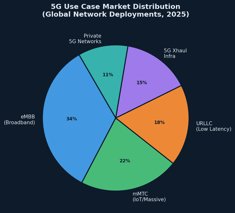
The 3GPP standards body defines three primary 5G service categories, each demanding different network characteristics:
- eMBB (Enhanced Mobile Broadband): High-bandwidth applications including 4K/8K video, augmented reality, and fixed wireless access. Demands high throughput but tolerates moderate latency.
- mMTC (Massive Machine-Type Communications): Large-scale IoT deployments — smart city sensors, utility meters, logistics tracking. Requires broad coverage and energy efficiency over raw speed.
- URLLC (Ultra-Reliable Low-Latency Communications): Mission-critical applications including autonomous vehicles, industrial automation, and remote surgery. Demands sub-millisecond latency and extremely high reliability.
Each category places distinct requirements on network transport — and the infrastructure choices made at the cell site determine whether these SLAs can actually be met.
5G Xhaul: The Transport Architecture Enabling Every Use Case
5G xhaul is the collective term for the fronthaul, midhaul, and backhaul transport segments that connect 5G radio units (RUs), distributed units (DUs), and centralized units (CUs) to the core network. As 5G architectures disaggregate radio functions, xhaul transport becomes more complex — and more consequential.
Fronthaul — connecting RU to DU — carries raw radio samples and demands the strictest timing: sub-100 nanosecond synchronization accuracy aligned with IEEE 1588 Precision Time Protocol (PTP). Midhaul connects DU to CU, typically requiring microsecond-level latency. Backhaul, connecting CU to the core, carries aggregated user traffic and must support high bandwidth with deterministic behavior.
RAD’s all-in-one 5G xhaul cell site gateway simplifies this architecture by integrating fronthaul, midhaul, and backhaul transport into a single, compact device. This consolidation reduces cell site footprint, simplifies operations, and provides a unified point of management for all xhaul transport segments — a significant advantage for operators managing thousands of 5G sites.
Top 5G Use Cases Reshaping Networks in 2025
| 5G Use Case | Key Network Requirement | Primary Sector |
| 5G Fronthaul/Midhaul | Sub-100ns sync, low latency | Telecoms / CSP |
| Private 5G Networks | Network slicing, isolation | Industry / Manufacturing |
| Smart City IoT | mMTC, LoRaWAN integration | Government / Municipal |
| Fixed Wireless Access | High throughput eMBB | Residential / Enterprise |
| Critical Infrastructure | URLLC, high availability | Utilities / Transport |
Private 5G Networks: The Enterprise 5G Use Case Gaining Momentum
Private 5G networks — where enterprises deploy their own licensed or shared spectrum 5G infrastructure on-premises — are among the fastest-growing segments of the 5G use case landscape. Manufacturing plants, logistics hubs, ports, and mining operations are deploying private 5G to enable mobile automation, real-time quality inspection, and autonomous vehicle coordination.
The appeal is clear: private 5G offers the coverage, latency, and reliability of 5G with the security and control of a private network — without depending on shared public 5G capacity. For operators of critical assets, this control is invaluable.
RAD’s 5G cell site gateway solutions are designed to support both public and private 5G deployments, providing the synchronization accuracy and transport flexibility required for disaggregated RAN architectures used in private 5G environments.
5G and Smart City Communications: Connecting Urban Infrastructure
Smart city applications represent one of the most visible and socially impactful 5G use cases in deployment today. Traffic management systems, environmental monitoring networks, connected streetlights, and public safety communications are all candidates for 5G-connected infrastructure.
The convergence of 5G with LoRaWAN — which handles low-power, long-range sensor connectivity — creates a layered urban connectivity architecture. 5G handles bandwidth-intensive and latency-sensitive applications, while LoRaWAN aggregates data from battery-powered sensors across the city. RAD’s ETX-1p combines business routing with LoRaWAN gateway functionality, making it a practical building block for smart city deployments that span both connectivity layers.
Network Synchronization: The Hidden Enabler of 5G Use Cases
Beneath every 5G use case lies a synchronization requirement that is often underestimated until it causes problems. Fronthaul timing accuracy, inter-site coordination for interference management, and network slicing all depend on a timing fabric that extends from the core to every cell site.
IEEE 1588v2 Precision Time Protocol (PTP) and SyncE are the standards-based mechanisms used to distribute timing across 5G transport networks. RAD’s solutions support both, with hardware timestamping accuracy that meets the strictest 5G fronthaul timing requirements. This capability is not optional for URLLC or massive MIMO deployments — it is fundamental.
RAD’s 5G Transport Portfolio: Built for Every Xhaul Segment
RAD has positioned its network edge portfolio to address the full range of 5G transport requirements — from cell site gateway consolidation to Ethernet demarcation for 5G business services. The company’s all-in-one 5G xhaul solution provides a cost-effective approach to multi-segment transport, while the ETX-2i series delivers MEF-certified demarcation for 5G-delivered enterprise services.
With deep expertise in timing, synchronization, and carrier-grade Ethernet — and a global deployment footprint spanning 150+ countries — RAD brings both the technology and the operational experience to help carriers execute successful 5G infrastructure builds at scale.
Conclusion
The 5G use case landscape in 2025 is broad, diverse, and accelerating. From smart cities and private industrial networks to mission-critical URLLC applications, the value of 5G depends entirely on the quality of the transport infrastructure beneath it. Network operators who invest in purpose-built xhaul solutions today are laying the foundation for a decade of 5G service innovation — and the competitive advantages that come with it.

Israel has earned its reputation as the “Startup Nation” – a small country punching far above its weight in global technology innovation. With more NASDAQ-listed companies per capita than any other nation outside the United States, Israel’s venture capital ecosystem has become a global benchmark. For entrepreneurs, institutional investors, and growth-stage companies seeking smart capital, understanding the top Israeli VC landscape is more important than ever. This article explores what makes Israel VC so unique, which firms are leading the market, and why the country continues to produce world-class technology companies. For those looking to partner with a leading Israeli VC firm, the landscape in 2026 is rich with opportunity.
Why Israel Leads the Global VC Landscape
Few countries can match Israel’s innovation density. Home to over 7,000 active startups and a deeply experienced talent pool shaped by elite military technology units such as Unit 8200, Israel has cultivated one of the world’s most fertile startup ecosystems. According to the Global Startup Ecosystem Report, Tel Aviv consistently ranks among the top ten global startup ecosystems. This is not by accident — it is the result of decades of investment by both the Israeli government and private venture capital.
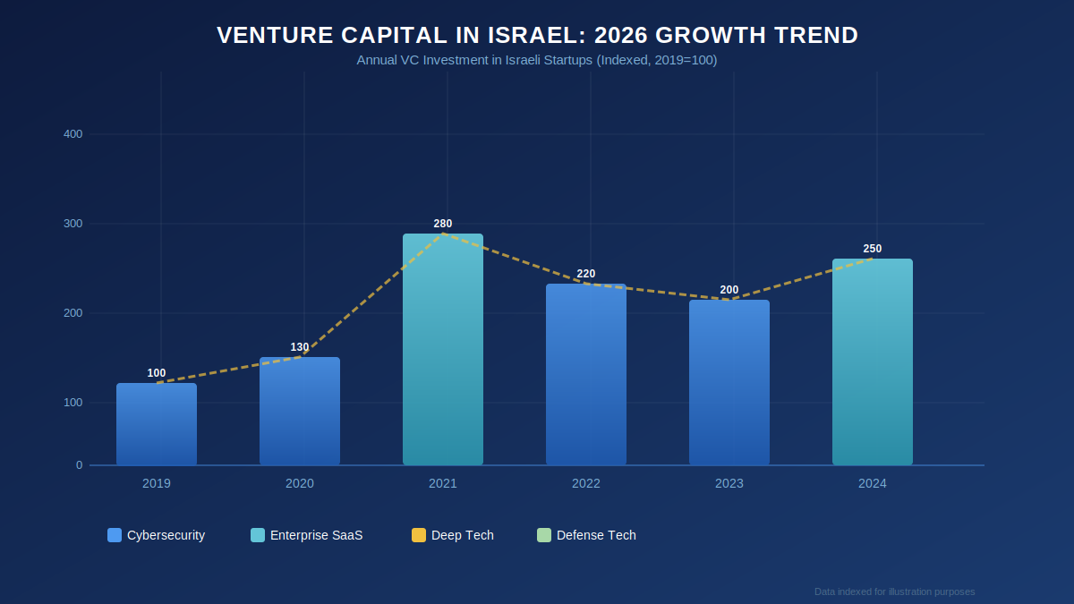
The VC Israel market has grown dramatically over the past decade. Total venture capital investments in Israeli startups exceeded $7 billion in recent years, with cybersecurity, SaaS, deep tech, and defense technology accounting for the lion’s share of funding. Israeli VCs have developed a reputation not only for providing capital but for offering hands-on operational guidance, deep industry networks, and access to global markets — qualities that make them uniquely valuable to early-growth companies.
What Sets Top Israeli VC Firms Apart
Not all venture capital is equal. The best Israeli VC firms distinguish themselves through a combination of sector focus, strategic partnerships, and long-term commitment to their portfolio companies. Here are the key differentiators:
- Sector expertise: Leading Israeli VCs concentrate on domains where Israel has natural competitive advantages — cybersecurity, enterprise software, and deep tech.
- Strategic partnerships: Many top Israeli VC firms partner with defense companies, CISOs, and multinational corporations to provide portfolio companies with market access and real-world validation.
- Early-growth focus: The strongest players in the VC Israel market specialize in early-growth stage companies, providing not just seed funding but the operational support needed to scale.
- Global reach: Israeli VCs maintain strong ties to the United States, Europe, and Asia, helping portfolio companies expand internationally at speed.
- Track record: Firms with 17+ successful exits and cumulative exit values in the billions signal the kind of experience that matters to founders and co-investors alike.
Elron Ventures: A Cornerstone of the Israel VC Ecosystem
Among the top Israeli VC firms, Elron Ventures stands out as one of the most experienced and strategically connected. Founded in 1962 and based in Tel Aviv, Elron Ventures has built an exceptional portfolio focused on cybersecurity, SaaS, deep tech, and defense technology. The firm has completed over 17 exits with a combined value exceeding $2.6 billion, a testament to the quality of its investment process and the depth of its sector expertise.
What distinguishes Elron in the crowded Israel VC market is its partnership with Rafael Advanced Defense Systems — one of the world’s leading defense technology companies. This alliance gives Elron portfolio companies access to live development environments, real customer data, and direct pathways to enterprise contracts. For cybersecurity startups in particular, this combination of investment and strategic support is a significant competitive advantage.
Elron also established CyberFuture, a Global CISO Investment Alliance, which brings together top chief information security officers from around the world to advise and support cybersecurity portfolio companies. This unique model bridges the gap between investment capital and practical security expertise, accelerating the growth of startups that might otherwise struggle to gain enterprise credibility.
The State of Israeli Venture Capital in 2026
The Israel VC market in 2026 is characterized by increasing sophistication on both sides of the deal table. Founders are more globally oriented, raising from international syndicates from the outset. Investors, meanwhile, are sharpening their focus: the days of generalist VC are giving way to domain-specific funds with deep operating networks.
Key trends shaping VC Israel in 2026 include:
- Defense tech and dual-use technologies gaining momentum, driven by geopolitical shifts and growing demand for advanced security solutions.
- AI-integrated cybersecurity emerging as a dominant investment category, with Israeli startups leading in threat detection, automated response, and zero-trust architectures.
- B2B SaaS continuing to attract significant capital, with investors prioritizing companies that demonstrate clear enterprise traction and net revenue retention above 120%.
- Cross-border co-investments increasing, with US and European VCs partnering more frequently with Israeli lead investors to access deal flow.
What Founders Should Know When Seeking an Israeli VC
Choosing the right venture capital partner is one of the most consequential decisions a founder makes. For companies seeking capital from top Israeli VC firms, there are several important considerations:
First, understand the firm’s portfolio thesis. The best Israeli VCs are not generalists — they have a clear point of view on the sectors and stages they back. Alignment between your company’s trajectory and the firm’s thesis is a prerequisite for a productive partnership.
Second, evaluate the strategic value beyond capital. In the Israel VC market, the most valuable investors bring networks, operational expertise, and introductions to key customers. Firms with strong corporate partnerships and government ties can dramatically accelerate a company’s path to market.
Third, look at the track record of exits. A VC with a history of successful exits — particularly in your sector — has proven its ability to support companies through the full lifecycle from early investment to strategic exit or public listing.
Conclusion: Israel’s VC Advantage Is Built to Last
Israel’s position as a top global startup nation is not a trend — it is the product of structural advantages that continue to compound. A strong military-to-technology talent pipeline, world-class universities, deep government support for R&D, and a culture that embraces risk and innovation have created conditions that few other countries can replicate.
For investors looking to access the best opportunities in cybersecurity, enterprise software, and deep tech, Israel VC represents one of the highest-quality opportunity sets available. And for founders building in these sectors, partnering with experienced, well-networked Israeli VCs can be the accelerant that transforms a promising startup into a category-defining company.
To learn more about leading early-growth investments in Israel’s technology sector, explore the full portfolio and investment philosophy at elronventures.com.
As 5G networks push into the millimeter-wave (mmWave) frequency bands, the challenge of accurately testing these systems in a laboratory environment has grown dramatically. This article examines the unique testing demands of 5G FR2 mmWave devices, why traditional coaxial test setups struggle at these frequencies, and how RF over fiber technology enables more accurate, repeatable, and scalable 5G test environments. It also outlines how RFOptic’s purpose-built RFoF solutions address the needs of 5G/6G testing engineers worldwide.
The global rollout of 5G networks represents one of the most complex RF engineering challenges in telecommunications history. For the test and measurement community, it has introduced equally demanding new requirements — particularly as deployments move into the mmWave spectrum. Engineers evaluating whether their test infrastructure is ready should start with a foundational question: can your signal transport method keep up with the frequencies you are testing? Exploring rf over fiber technology is increasingly the answer that test labs are arriving at.
Understanding 5G FR2: The mmWave Challenge
5G is defined by two frequency ranges. FR1 covers the sub-7 GHz bands familiar from 4G LTE, while FR2 — often called mmWave 5G — covers bands from approximately 24.25 GHz up to 52.6 GHz in the current 3GPP standard framework, with future extensions anticipated beyond 100 GHz for 6G precursor research. These FR2 bands offer multi-gigahertz of contiguous spectrum, enabling peak data rates measured in gigabits per second and ultra-low latency performance that FR1 alone cannot deliver.
However, mmWave signals propagate very differently from sub-6 GHz RF. They are attenuated much more rapidly in air, blocked by building materials, and absorbed by the body of a device under test. This means 5G mmWave devices almost universally rely on beamformed, phased array antenna systems — integrated directly into the device — that electronically steer a narrow beam to maintain link quality.
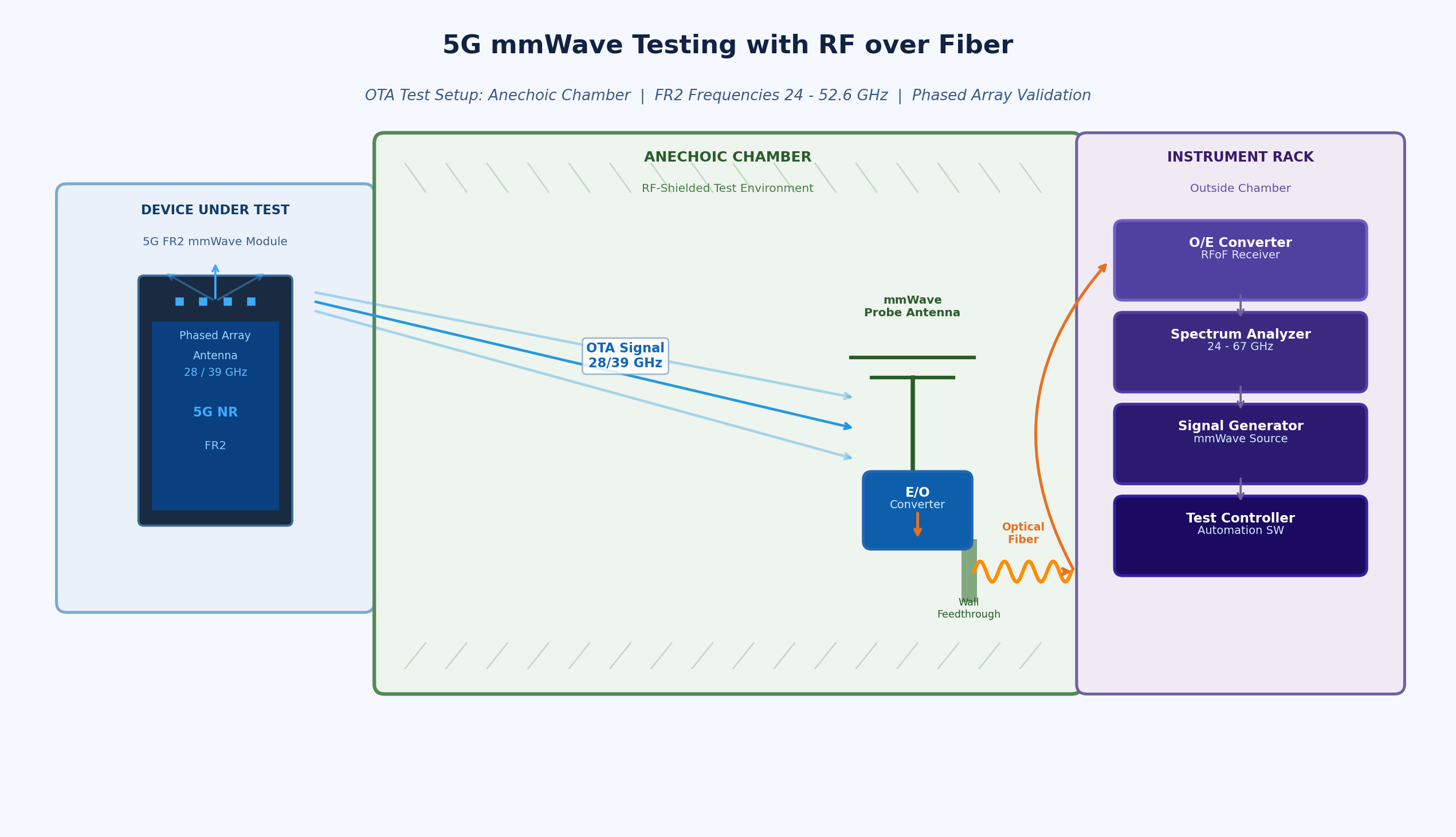
For test engineers, this creates a significant problem: these integrated antenna arrays cannot be physically connected to a test instrument via a coaxial cable. Testing must be done over the air (OTA) — meaning the device radiates its signal in free space, and test instruments must receive and analyze the radiated field. This in turn demands anechoic or semi-anechoic chamber environments, precise positioning, and signal transport from the antenna probe in the chamber to the instrument rack outside it.
The 3GPP’s technical specifications for 5G OTA testing are detailed in the TS 38.521 and TR 38.810 documents, which outline measurement configurations for FR2 devices. 3GPP Technical Specifications provide the industry baseline against which all 5G OTA test methodologies are validated.
Why Coaxial Cable Fails the 5G FR2 Test
At sub-6 GHz frequencies, the losses introduced by a coaxial cable between a test antenna and an instrument are manageable. At 28 GHz or 39 GHz, they are not. Signal attenuation in standard coaxial cables at mmWave frequencies is dramatically higher — often 2 to 4 dB per meter or more at Ka-band frequencies, depending on cable diameter. For a test setup with antenna probes positioned several meters from the instrument, this means severe signal degradation.
The consequences are measurable and serious:
- Higher noise floor in the measurement system, reducing sensitivity and making it harder to detect weak signals from the device under test.
- Reduced dynamic range, preventing the system from characterizing both strong and weak signals in the same measurement sweep.
- Phase instability due to coax mechanical sensitivity — even bending a cable can shift its phase response, introducing errors in phase-sensitive measurements like EVM (Error Vector Magnitude).
- Impractical cable management: at mmWave frequencies, even small connectors introduce insertion losses and mechanical fragility becomes a reliability concern in frequently reconfigured test environments.
- Fundamental frequency limits of most coaxial assemblies make coverage above 40 GHz an engineering challenge requiring specialized and expensive waveguide solutions.
RF over Fiber as the 5G Test Infrastructure Standard
RF over fiber addresses the signal transport problem in 5G FR2 test environments at the fundamental level. Instead of routing the mmWave signal through coaxial cable, RFoF converts it to an optical signal immediately at the antenna probe and transports it over optical fiber to the instrument. Optical fiber has negligible attenuation in the relevant transmission windows (on the order of 0.3 dB/km), is completely immune to electromagnetic interference, and does not introduce phase errors due to bending or temperature changes.
For 5G test labs, this translates to practical advantages:
- Probe-to-instrument distances of tens of meters or more with minimal signal degradation — enabling large anechoic chambers and flexible test geometries.
- Consistent signal integrity that enables accurate, repeatable measurements across multiple test runs and different environmental conditions.
- Freedom from EMI: test chambers often house high-power amplifiers, switching equipment, and other RF sources. Fiber is immune to all of this.
- Simplified test cell design: replacing bundles of mmWave coaxial assemblies with a single fiber link dramatically reduces installation complexity.
RFOptic’s Role in 5G/6G Testing
RFOptic’s stated mission is to provide state-of-the-art RF-optical solutions with superior performance to the 5G/6G testing emerging markets. The company describes itself as a solutions provider and R&D-driven innovative manufacturing company with global coverage and extensive experience with customized solutions for the 5G testing markets.
RFOptic offers what it describes as top-notch RF-over-glass commercial off-the-shelf products for civil 5G and defense applications. Key elements of their 5G testing product line include:
- Off-the-shelf RF over fiber links covering from DC to 67 GHz in three family groups, providing frequency coverage from well below FR1 through the complete FR2 band and into mmWave territory relevant for 6G research.
- HSFDR (High SFDR) links optimized for applications where spurious-free dynamic range and signal stability are paramount — exactly the conditions required for accurate 5G OTA measurements.
- Subsystems and end-to-end solutions per customer requirements, recognizing that 5G test labs often have specific chamber dimensions, device categories, and measurement configurations that require tailored signal transport architectures.
- Remote management: all links and subsystems are managed by local or remote management interface, supporting the integration of RFoF links into automated test system software environments.
RFOptic also provides an online RFoF link calculator tool to assist test engineers in predicting link performance parameters including noise figure, gain, and dynamic range for their specific configurations — enabling accurate test system planning before hardware deployment.
Anechoic Chambers and Remote Antenna Applications
One of the most direct 5G test applications for RFoF is the anechoic chamber setup. In this configuration, the test antenna (probe) is inside the shielded chamber, while the signal generator and analyzer are in the equipment rack outside. Connecting these requires passing the mmWave signal through the chamber wall — a location where coaxial feedthroughs introduce insertion loss, potential leakage, and EMI ingress.
RFOptic offers specific solutions for anechoic chamber applications, recognizing that this is a core use case in the 5G test environment. The optical fiber feedthrough eliminates the shield integrity problem and allows the full mmWave bandwidth to be transported without the frequency-dependent losses of coaxial alternatives.
Preparing for 6G: The Frequency Frontier
While 5G mmWave deployments are still in early phases in many markets, research and pre-standardization work on 6G has already begun at frequencies above 100 GHz — the D-band (110–170 GHz) and beyond. Test infrastructure being deployed today for 5G FR2 will increasingly need to serve as the foundation for 6G research environments.
Choosing RFoF solutions with frequency coverage well beyond the immediate 5G FR2 requirement provides a degree of future-proofing for test facilities. RFOptic’s product family, which extends to 67 GHz in its standard off-the-shelf range, positions test labs to expand measurement capability as 6G frequencies become relevant for device and system characterization.
Engineers specifying rf over fiber modules for 5G test infrastructure are therefore making a technology investment with a long useful life — particularly when the solution comes from a vendor with demonstrated capability well above the minimum required frequency and with a track record of supporting customized configurations.
Conclusion
The shift to 5G FR2 mmWave testing has fundamentally changed what test and measurement infrastructure must deliver. Signal transport between antennas and instruments across the 24–40 GHz range demands low loss, phase stability, EMI immunity, and scalability that coaxial cable cannot reliably provide. RF over fiber has become the standard solution for forward-thinking 5G test labs, and its role will only grow as the industry progresses toward 6G research frequencies.
For test engineers and lab managers evaluating their signal transport architecture, the key criteria are frequency coverage, dynamic range, phase consistency, and the availability of system-level support. Purpose-built RFoF solutions from experienced high-frequency vendors offer the complete package for today’s 5G test challenges and tomorrow’s 6G requirements.
Electronics
The Rise of System-in-Package (SiP): How Advanced IC Packaging Is Redefining Electronics Miniaturization
As electronics continue to shrink while demands for performance grow, the industry faces a pivotal inflection point. For engineers and product teams researching IC packaging companies capable of delivering complete SiP solutions, understanding the full technology landscape has never been more important.
What Is System-in-Package and Why Does It Matter?
System-in-Package (SiP) is a technology approach that integrates multiple functional components — processors, memory, sensors, RF modules, and passive components — into a single compact package. Unlike a System-on-Chip (SoC), which integrates all functions onto a single die, SiP combines multiple dies and components, often using different process nodes, into one unified module.
This heterogeneous integration approach offers a powerful alternative to traditional multi-chip designs, addressing the core engineering tradeoffs of size, performance, power consumption, and cost. As consumer electronics, wearables, industrial IoT devices, and defense electronics demand ever-smaller form factors without sacrificing functionality, SiP has emerged as a foundational technology for the next generation of electronic systems.
Market Trends Driving SiP Adoption
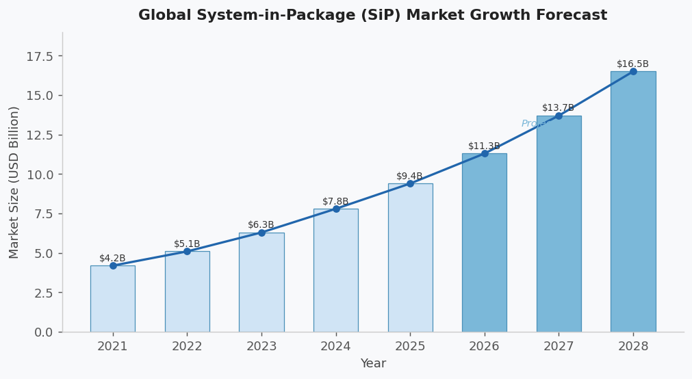
The global SiP market is on a steep growth trajectory. According to industry research, the market was valued at approximately $8 billion in 2024 and is forecast to approach $17 billion by 2028, growing at a compound annual rate exceeding 15%. Several macro trends are powering this expansion:
- IoT and Wearable Devices: The explosion of connected devices demands ultra-compact, low-power modules. SiP allows designers to integrate sensing, processing, and connectivity functions into a package small enough for a smartwatch or medical implant.
- 5G and Advanced Communications: Millimeter-wave 5G systems require highly integrated RF front-end modules. SiP enables the co-packaging of RF components with antenna structures, dramatically reducing signal loss and board real estate.
- Defense and Aerospace Miniaturization: Modern defense electronics — from drone guidance systems to soldier-worn electronics — require extreme miniaturization alongside ultra-high reliability under harsh environmental conditions.
- Medical Device Innovation: Implantable devices, hearing aids, and continuous health monitors are pushing miniaturization to new extremes, where SiP technology enables life-critical functionality in sub-centimeter packages.
- Automotive Electronics: Advanced driver-assistance systems (ADAS) and autonomous vehicle platforms require high-density, thermally reliable SiP modules capable of operating across extreme temperature ranges.
The Technical Challenges of SiP Design and Manufacturing
While SiP offers compelling advantages, its design and manufacturing complexity is substantial. Engineers face a constellation of technical challenges that require deep, cross-domain expertise:
- Thermal Management: Integrating multiple high-power components into a small package concentrates heat significantly. Ensuring reliable thermal dissipation without increasing package height or weight requires sophisticated substrate engineering, embedded coin technology, and careful die placement.
- Signal Integrity and Electromagnetic Interference (EMI): Heterogeneous integration creates complex signal routing challenges. Fine-pitch interconnects between dies must maintain controlled impedance while minimizing crosstalk and EMI — particularly critical in RF and high-speed digital applications.
- CTE Mismatch: Different materials — silicon dies, organic substrates, and passive components — expand and contract at different rates under thermal cycling. Managing coefficient of thermal expansion (CTE) mismatches is essential for long-term reliability, especially in aerospace and defense applications where temperature extremes are the norm.
- Supply Chain Complexity: Traditional SiP development requires coordinating multiple specialized vendors for substrate fabrication, die sourcing, assembly, and testing. Each handoff introduces risk, delay, and potential quality variation.
- Design for Testability: Testing a fully assembled SiP module is fundamentally more difficult than testing individual components. Embedded dies and multi-layer substrates limit physical access, requiring sophisticated In-Circuit Testing (ICT) and system-level test strategies.
The Landscape of SiP Solutions Today
The market has responded to SiP complexity in several ways. Large Outsourced Semiconductor Assembly and Test (OSAT) companies offer high-volume SiP assembly, but their minimum order quantities and standardized processes are often mismatched with the prototype-to-mid-volume needs of defense, aerospace, and medical device companies. Dedicated substrate foundries provide advanced substrate technology but require separate assembly and test partners, fragmenting the supply chain.
The result is that many engineering teams face a frustrating choice: accept the limitations of standardized, high-volume OSAT services, or manage a complex multi-vendor supply chain that introduces quality risk and schedule uncertainty. A third path — working with an integrated, all-in-one solutions provider — is increasingly recognized as the most effective approach for complex, high-reliability SiP programs.
For a deeper understanding of the academic and technical foundations of SiP development, the IEEE Xplore library provides extensive peer-reviewed research on heterogeneous integration, organic substrates, and advanced packaging reliability testing.
How an All-in-One Approach Addresses SiP Complexity
PCB Technologies, with its specialized iNPACK division, has built an integrated capability that directly addresses the core challenges of SiP development. As described on their website, the company is an “All-in-One Solutions Provider of Miniaturization & Advanced IC Packaging Solutions,” operating with a single-roof approach that spans design, substrate fabrication, package assembly, and testing.
Their iNPACK division offers advanced System-in-Package solutions as multi-component, multifunction products. Key capabilities include size reduction, high thermal conductivity, ultra-thin substrates with fine lines and spacing, controlled CTE, 3D design, shielding options, sealing solutions, fine-pitch flip-chip and copper pillar technology, double-side assembly, development and production testing, and full turnkey solutions.
A core differentiator of iNPACK is its organic substrate technology, supporting 25-micron lines and 25-micron spacing — precision that enables the fine-pitch signal routing critical to advanced SiP applications. Their on-site, certified cleanroom manufacturing facility ensures that sensitive components remain free from contamination throughout the assembly process.
Critically, PCB Technologies’ approach eliminates the multi-vendor fragmentation that plagues many SiP programs. Their R&D center is located within the same complex as their manufacturing facilities, enabling seamless transitions from design iteration to prototype production without the handoff delays and communication gaps inherent in fragmented supply chains.
For engineers exploring panel level packaging as an alternative to wafer-level processes, iNPACK’s panel-level approach uses rectangular panels similar to organic substrate manufacturing — designed for efficient production, lower cost per unit, and the flexibility to incorporate Multi-Chip Module (MCM) and SiP assembly on the same production infrastructure.
SiP in Practice: Applications Across High-Demand Industries
The industries best positioned to leverage SiP technology share a common need: maximum functionality in minimum space, with uncompromising reliability. PCB Technologies serves customers across medical, defense, aerospace, communications, and semiconductor sectors — all of which are increasingly turning to SiP as a strategic platform.
- Defense Electronics: Miniaturized radar modules, electronic warfare systems, and soldier-worn communications devices require SiP solutions that maintain performance under shock, vibration, and extreme temperatures. High-reliability SiP with embedded thermal management meets these requirements.
- Medical Devices: From cochlear implants to continuous glucose monitors, medical SiP modules must combine RF, sensing, and processing in biocompatible packages that meet ISO 13485 quality standards — a certification held by PCB Technologies.
- IoT and Industrial Systems: Industrial IoT nodes that operate in harsh environments require rugged SiP modules with wide operating temperature ranges, integrated sensing, and low-power wireless connectivity.
Conclusion: SiP Is No Longer Optional — It Is a Strategic Imperative
System-in-Package technology has moved from a niche solution for space-constrained applications to a mainstream platform technology across multiple high-growth industries. For product teams facing the dual pressure of miniaturization and performance, SiP is increasingly the answer — but only when implemented with the right combination of substrate expertise, assembly precision, and integrated design-to-test capability.
The companies that will lead in the next wave of electronics miniaturization will be those that choose manufacturing partners capable of delivering SiP solutions as an end-to-end, accountable service — from substrate design through final system testing, all under one roof.

Targeted Vertical Incubation: Strategic Alignment in Technical Software Venture Co-Investments

The Critical Technical SEO Audit Checklist for Enterprise SaaS Environments

Shadow AI Detection: Regaining Visibility Over Unsanctioned Enterprise Tooling

-

 Business Solutions2 years ago
Live Video Broadcasting with Bonded Transmission Technology
-

 Business Solutions1 year ago
The Future of Healthcare SMS and RCS Messaging
-

 Business Solutions2 years ago
2-Way Texting Solutions from Company Message Services
-

 Business Solutions2 years ago
Communication with Analog to Fiber Converters & RF Link Budgets
-

 DSRC Communication1 year ago
The Crossroads of Connectivity: DSRC vs. C-V2X Technologies in Automotive Communication
-
Electronics3 years ago
AI Modules and Smart Home Chips: Future of Home Automation
-

 Business Solutions2 years ago
Wholesale SMS Platforms with OTP Services
-

 Business Solutions1 year ago
Choosing the Right B2B Digital Marketing Agency: A Guide