


Electronics
Programmable Power Supplies And their Various Benefits

You might be planning a big launch of your new product very soon that you think can turn your career around for the best. You’ve probably been working on your project for months or maybe years. You’re high with anticipation and excitement as only the last step is remaining – the testing part of your promising next-gen technology. You’re on the verge of success and all you need is that power supply to do the testing.
The road to success is never an easy one but when you have powerful allies, it will become a little easier to traverse along that rocky road. In your case, your last hurdle to cross is the power supply which is easy to overcome with a reliable programmable power supply.
However, there are so many companies in the market that claim to offer the best quality products but in reality, most of them are substandard and cost way too much. That’s why you should be cautious about choosing a programmable power supplier. Here’s what you should expect in a best-in-class programmable power supply.
Customize Them to Your Will
Any high quality extended range programmable power supply will be customizable. For greater precision in the power supply, the unit should give you more control over the power output. The standard power supply input won’t be able to handle your next-gen tech and for that, you need an upgraded extended range programmable DC power supply. You will need to increase and decrease the power supply to test out the equipment and for that, you will need a flexible power supply unit that can provide any power demand as per your requirement.
Apart from that, if the power supply unit is not stable enough then your equipment is sure to suffer damage. Therefore, look for a perfect combination of built-in voltage and current measurement, panel control that can be locked to prevent any unforeseen changes and a stable output so that you have greater freedom and precision in testing your product. Any extended-range power supply system will come with the additional benefit of over-voltage, over-temperature and over-electric current protection for your equipment by limiting the current output or shutting down entirely.
Like It Isn’t Even There
Choose a power supply unit that perfectly fits in a corner. If you are working on a big project, it’s highly likely that you’ll have a lot of clutter scattered around in your workshop. It’s already hard to fit in all the instruments in your garage; can you really afford to include a gargantuan power supply unit with a million different units that take up a lot of space? That’s why opt for a power supply unit that is small and compact. A good power supply unit will quietly work in a corner like it isn’t even there!
Money Matters!
You have already spent a lot of money developing your dream project –you don’t want to compromise with the quality! But developing the product is only the beginning of the journey and there is still a lot more to do which requires money. You’ll need to cut down on your budget to save for later developments. Luckily, many good companies are now offering a programmable power supply unit that not only offers great power output but also at a reasonable price. This way you don’t have to wreck your brain over how to balance quality and cost. It’s possible to get a high-quality power supply system at an affordable price so don’t let money stop your progress!
Be Ahead Of Time
Get the extended range power supply before it becomes main-stream! The flexible and stable output along with safety measures, affordable price and space conservative nature of this power supply system has already made it unmatched in the market. It is bound to become the undisputed king of power suppliers with all the attention it has been receiving from engineers. You can stay ahead in the game with this next-gen programmable DC power supply for your next-gen product!
There you go! This guide should help you find the best power supply unit for your project. Now you can achieve all the success with this powerfully!

programmable power supply


Buildings, tunnels, and parking structures block GPS satellite signals from reaching the devices that depend on them for precise timing. Distributing a single rooftop GPS signal to many indoor locations without losing accuracy is a common, and often underestimated, engineering problem. This piece walks through how GPS over fiber distribution solves it, in plain question-and-answer form.
Why can’t you just run coax to every timing device?
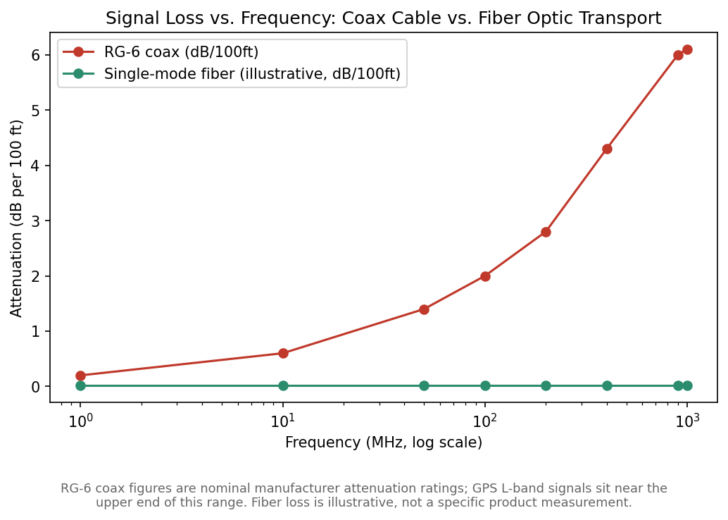
Coaxial cable loses signal strength as it gets longer, and that loss gets worse at higher frequencies. GPS signals sit up near 1.5 GHz, a range where coax attenuation climbs quickly. Once a cable run stretches beyond roughly a hundred feet, the accumulated loss can degrade the signal below what a receiver needs to lock onto it reliably.
Nominal coax attenuation rises steeply with frequency, while fiber optic loss stays comparatively flat and low (illustrative, not a specific product measurement).
How does the fiber-based alternative work?
A rooftop GPS antenna feeds a transmitter module that converts the incoming satellite signal onto an optical carrier. That optical signal travels over low-loss fiber, and can be split to reach many destinations at once using standard optical splitters, before a fiber optic transmitter and receiver pair converts each branch back to an RF GPS signal at its endpoint. Because a single donor antenna can feed dozens of splits, one rooftop receiver can serve timing devices scattered across an entire facility.
What actually needs this kind of precise timing?
Data centers rely on GPS timing to keep distributed systems synchronized. Financial networks use it to timestamp transactions consistently across locations. Highway tunnels sometimes need GPS re-radiated inside for emergency vehicle navigation. In each case the requirement is the same: get an accurate, undistorted GPS signal to a location the satellite signal itself can’t reach directly.
How precise does GPS timing actually get?
According to the U.S. government’s official GPS information site, GPS time transfer is commonly used to synchronize clocks and networks to Coordinated Universal Time, with a typical accuracy relative to the U.S. Naval Observatory’s time standard of 30 nanoseconds or better, 95 percent of the time, when using a dedicated time-transfer receiver. See GPS.gov’s overview of GPS timing applications for more detail on how that precision is used across industries.
Frequently Asked Questions
Why does GPS signal distribution need fiber instead of just more coax?
Coax loss increases sharply at GPS frequencies, so runs longer than about a hundred feet start to degrade signal quality. Fiber optic loss stays low over much longer distances.
Can one GPS antenna really serve an entire building?
Yes. Once the signal is converted to an optical carrier, it can be split many times using standard optical splitters, letting a single rooftop antenna feed numerous indoor endpoints.
What industries rely most on distributed GPS timing?
Data centers, financial networks, and telecommunications infrastructure are common users, since all depend on precise, synchronized time across multiple locations.
Among the most widely used IC packages in modern electronics, QFN packages have earned their place in product designs ranging from Bluetooth chips to automotive radar modules. Compact, thermally efficient, and electrically clean, QFN (Quad Flat No-Lead) packages offer a compelling combination of performance and manufacturability. But not all QFN packages are equal — and the differences between standard, organic, and panel-level variants can significantly affect both product performance and production economics.
This article breaks down the key QFN package types, explores their respective advantages, and explains how advances in panel-level packaging are reshaping the economics of high-volume production.
What Is a QFN Package?
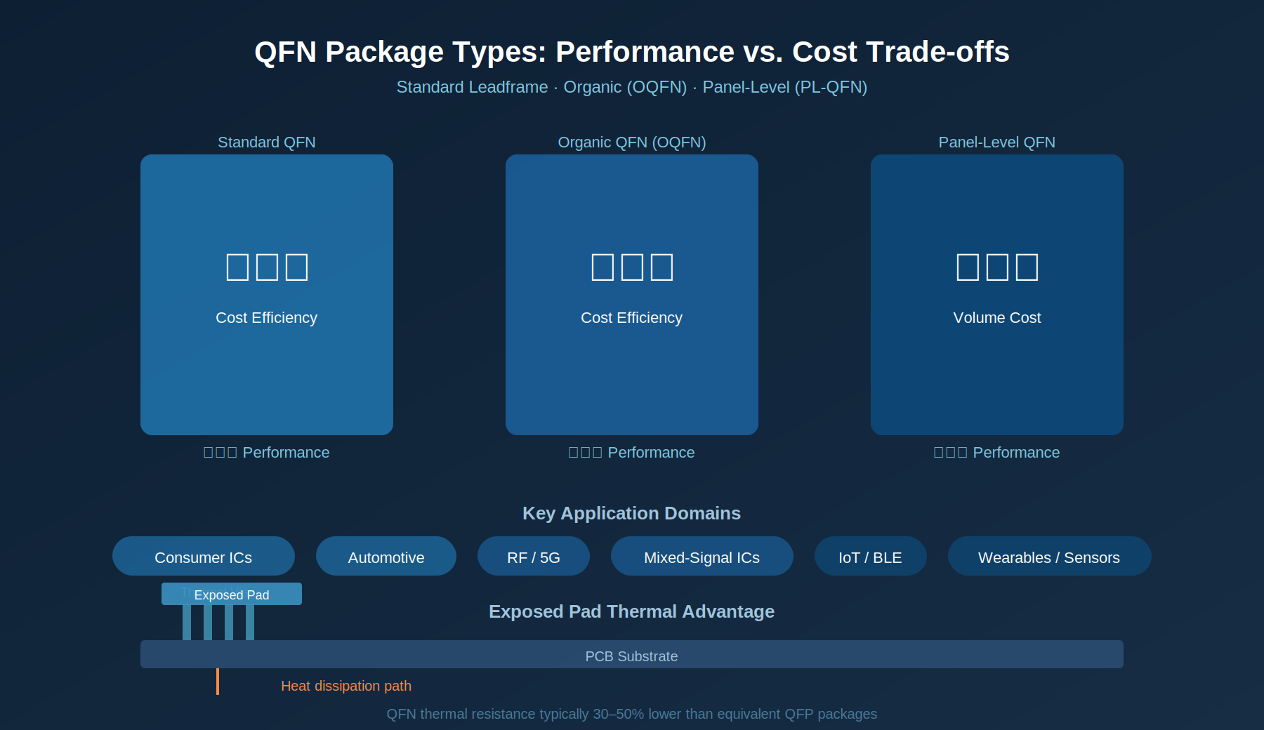
QFN stands for Quad Flat No-Lead — a surface-mount package format where leads are located on the underside of the package rather than extending outward. A large exposed pad on the package bottom provides a direct thermal path to the PCB, making QFN one of the most thermally efficient small-form-factor package types available.
The absence of external leads reduces parasitic inductance and capacitance compared to gull-wing leaded packages, improving high-frequency performance. This combination of thermal and electrical benefits has made QFN the package of choice across consumer electronics, wireless communications, industrial sensors, and automotive control units.
QFN Package Types: A Comparison
While the QFN concept is consistent, several variants have emerged to serve different manufacturing processes and performance requirements:
| Package Variant | Process Basis | Key Advantage | Typical Use |
| Standard QFN | Leadframe + molding | Low cost, mature supply chain | Consumer ICs, PMIC |
| Organic QFN (OQFN) | Organic substrate | Finer pitch, better signal integrity | RF, telecom, mixed-signal |
| Panel-Level QFN (PL-QFN) | Panel-level packaging | Ultra-low cost at volume | IoT, wearables, automotive |
| Dual-Row QFN | Leadframe | Higher I/O density | Connectivity ICs |
| Thermally Enhanced QFN | Leadframe + thermal slug | Superior heat dissipation | Power semiconductors |
Organic QFN: The High-Performance Alternative
Traditional QFN packages use a metal leadframe as the substrate — a cost-effective approach that suits high-volume commodity ICs. Organic QFN replaces the leadframe with an organic laminate substrate, enabling finer pitch routing, better impedance control, and improved electrical performance for RF and mixed-signal applications.
For RF front-end modules, millimeter-wave components, and precision analog ICs, organic QFN delivers performance characteristics that leadframe-based packages cannot match. The substrate enables multi-layer routing, embedded passive integration, and support for tighter pad pitches demanded by advanced silicon nodes.
PCB Technologies’ iNPACK division has developed deep capabilities in organic QFN manufacturing, offering DFM consultation, rapid prototyping, and scalable production. Their approach ensures that performance-optimized designs translate successfully from simulation to silicon.
Panel-Level Packaging: The Cost Revolution
Wafer-level packaging has long been the benchmark for cost-efficient IC packaging in high-volume production — but it is constrained by wafer diameter. Panel-level packaging applies the same lithographic and encapsulation processes to rectangular panels many times larger than a 300mm wafer, dramatically increasing throughput per equipment cycle.
For QFN-type packages produced at scale, panel-level processing can reduce per-unit cost by 30–50% compared to wafer-level equivalents, depending on die size and panel utilization. This cost structure is transforming the economics of IoT components, wireless modules, and automotive sensor ICs — categories where per-unit price pressure is intense.
Thermal Management in QFN Designs
One of the most critical design decisions when using QFN packages is thermal management at the board level. The exposed thermal pad requires careful PCB design to maximize heat transfer:
- Thermal via arrays beneath the exposed pad are strongly recommended for high-power devices
- Pad size should follow IPC-7351 land pattern guidelines for the specific package
- Solder paste aperture design affects both electrical connection and thermal conductivity
- Adjacent ground planes and copper pours help spread heat away from the die
Poor thermal design with QFN packages can negate their inherent thermal advantage, resulting in premature failure or derating. PCB Technologies provides DFM review as part of their packaging engagement, catching thermal design issues before they reach prototype stage.
QFN vs. QFP: When Each Makes Sense
The most common comparison made against QFN is QFP (Quad Flat Package) — the leaded alternative. Each format has its place:
- QFN: Better for high-frequency applications, tighter board area budgets, and superior thermal performance; requires precision solder printing
- QFP: Easier to inspect visually and rework, more forgiving of PCB assembly tolerances; larger footprint
For new designs targeting advanced nodes and compact form factors, QFN consistently wins the performance-per-area tradeoff. The manufacturing challenge of QFN — particularly solder void management under the thermal pad — is well-understood and manageable with proper process controls.
PCB Technologies’ QFN Capability
PCB Technologies offers end-to-end QFN packaging services through their iNPACK platform, spanning design consultation, substrate development, packaging, and test. Their organic QFN capabilities support pitches not achievable with standard leadframe-based processes, making them a strong partner for next-generation wireless, automotive, and medical IC designs.
With established supply chains for organic substrate materials and a track record across demanding qualification standards, PCB Technologies bridges the gap between the cost efficiency demanded by volume production and the performance requirements of advanced applications.
Conclusion
QFN packages continue to evolve — from standard leadframe variants to organic and panel-level formats that unlock new performance and cost tiers. As silicon advances drive smaller die sizes and higher I/O densities, the packaging layer becomes increasingly critical. Selecting the right QFN variant and working with an experienced packaging partner ensures that board-level performance matches the potential of the silicon within.
Electronics
The Rise of System-in-Package (SiP): How Advanced IC Packaging Is Redefining Electronics Miniaturization

As electronics continue to shrink while demands for performance grow, the industry faces a pivotal inflection point. For engineers and product teams researching IC packaging companies capable of delivering complete SiP solutions, understanding the full technology landscape has never been more important.
What Is System-in-Package and Why Does It Matter?
System-in-Package (SiP) is a technology approach that integrates multiple functional components — processors, memory, sensors, RF modules, and passive components — into a single compact package. Unlike a System-on-Chip (SoC), which integrates all functions onto a single die, SiP combines multiple dies and components, often using different process nodes, into one unified module.
This heterogeneous integration approach offers a powerful alternative to traditional multi-chip designs, addressing the core engineering tradeoffs of size, performance, power consumption, and cost. As consumer electronics, wearables, industrial IoT devices, and defense electronics demand ever-smaller form factors without sacrificing functionality, SiP has emerged as a foundational technology for the next generation of electronic systems.
Market Trends Driving SiP Adoption
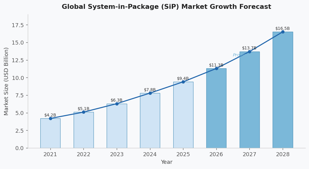
The global SiP market is on a steep growth trajectory. According to industry research, the market was valued at approximately $8 billion in 2024 and is forecast to approach $17 billion by 2028, growing at a compound annual rate exceeding 15%. Several macro trends are powering this expansion:
- IoT and Wearable Devices: The explosion of connected devices demands ultra-compact, low-power modules. SiP allows designers to integrate sensing, processing, and connectivity functions into a package small enough for a smartwatch or medical implant.
- 5G and Advanced Communications: Millimeter-wave 5G systems require highly integrated RF front-end modules. SiP enables the co-packaging of RF components with antenna structures, dramatically reducing signal loss and board real estate.
- Defense and Aerospace Miniaturization: Modern defense electronics — from drone guidance systems to soldier-worn electronics — require extreme miniaturization alongside ultra-high reliability under harsh environmental conditions.
- Medical Device Innovation: Implantable devices, hearing aids, and continuous health monitors are pushing miniaturization to new extremes, where SiP technology enables life-critical functionality in sub-centimeter packages.
- Automotive Electronics: Advanced driver-assistance systems (ADAS) and autonomous vehicle platforms require high-density, thermally reliable SiP modules capable of operating across extreme temperature ranges.
The Technical Challenges of SiP Design and Manufacturing
While SiP offers compelling advantages, its design and manufacturing complexity is substantial. Engineers face a constellation of technical challenges that require deep, cross-domain expertise:
- Thermal Management: Integrating multiple high-power components into a small package concentrates heat significantly. Ensuring reliable thermal dissipation without increasing package height or weight requires sophisticated substrate engineering, embedded coin technology, and careful die placement.
- Signal Integrity and Electromagnetic Interference (EMI): Heterogeneous integration creates complex signal routing challenges. Fine-pitch interconnects between dies must maintain controlled impedance while minimizing crosstalk and EMI — particularly critical in RF and high-speed digital applications.
- CTE Mismatch: Different materials — silicon dies, organic substrates, and passive components — expand and contract at different rates under thermal cycling. Managing coefficient of thermal expansion (CTE) mismatches is essential for long-term reliability, especially in aerospace and defense applications where temperature extremes are the norm.
- Supply Chain Complexity: Traditional SiP development requires coordinating multiple specialized vendors for substrate fabrication, die sourcing, assembly, and testing. Each handoff introduces risk, delay, and potential quality variation.
- Design for Testability: Testing a fully assembled SiP module is fundamentally more difficult than testing individual components. Embedded dies and multi-layer substrates limit physical access, requiring sophisticated In-Circuit Testing (ICT) and system-level test strategies.
The Landscape of SiP Solutions Today
The market has responded to SiP complexity in several ways. Large Outsourced Semiconductor Assembly and Test (OSAT) companies offer high-volume SiP assembly, but their minimum order quantities and standardized processes are often mismatched with the prototype-to-mid-volume needs of defense, aerospace, and medical device companies. Dedicated substrate foundries provide advanced substrate technology but require separate assembly and test partners, fragmenting the supply chain.
The result is that many engineering teams face a frustrating choice: accept the limitations of standardized, high-volume OSAT services, or manage a complex multi-vendor supply chain that introduces quality risk and schedule uncertainty. A third path — working with an integrated, all-in-one solutions provider — is increasingly recognized as the most effective approach for complex, high-reliability SiP programs.
For a deeper understanding of the academic and technical foundations of SiP development, the IEEE Xplore library provides extensive peer-reviewed research on heterogeneous integration, organic substrates, and advanced packaging reliability testing.
How an All-in-One Approach Addresses SiP Complexity
PCB Technologies, with its specialized iNPACK division, has built an integrated capability that directly addresses the core challenges of SiP development. As described on their website, the company is an “All-in-One Solutions Provider of Miniaturization & Advanced IC Packaging Solutions,” operating with a single-roof approach that spans design, substrate fabrication, package assembly, and testing.
Their iNPACK division offers advanced System-in-Package solutions as multi-component, multifunction products. Key capabilities include size reduction, high thermal conductivity, ultra-thin substrates with fine lines and spacing, controlled CTE, 3D design, shielding options, sealing solutions, fine-pitch flip-chip and copper pillar technology, double-side assembly, development and production testing, and full turnkey solutions.
A core differentiator of iNPACK is its organic substrate technology, supporting 25-micron lines and 25-micron spacing — precision that enables the fine-pitch signal routing critical to advanced SiP applications. Their on-site, certified cleanroom manufacturing facility ensures that sensitive components remain free from contamination throughout the assembly process.
Critically, PCB Technologies’ approach eliminates the multi-vendor fragmentation that plagues many SiP programs. Their R&D center is located within the same complex as their manufacturing facilities, enabling seamless transitions from design iteration to prototype production without the handoff delays and communication gaps inherent in fragmented supply chains.
For engineers exploring panel level packaging as an alternative to wafer-level processes, iNPACK’s panel-level approach uses rectangular panels similar to organic substrate manufacturing — designed for efficient production, lower cost per unit, and the flexibility to incorporate Multi-Chip Module (MCM) and SiP assembly on the same production infrastructure.
SiP in Practice: Applications Across High-Demand Industries
The industries best positioned to leverage SiP technology share a common need: maximum functionality in minimum space, with uncompromising reliability. PCB Technologies serves customers across medical, defense, aerospace, communications, and semiconductor sectors — all of which are increasingly turning to SiP as a strategic platform.
- Defense Electronics: Miniaturized radar modules, electronic warfare systems, and soldier-worn communications devices require SiP solutions that maintain performance under shock, vibration, and extreme temperatures. High-reliability SiP with embedded thermal management meets these requirements.
- Medical Devices: From cochlear implants to continuous glucose monitors, medical SiP modules must combine RF, sensing, and processing in biocompatible packages that meet ISO 13485 quality standards — a certification held by PCB Technologies.
- IoT and Industrial Systems: Industrial IoT nodes that operate in harsh environments require rugged SiP modules with wide operating temperature ranges, integrated sensing, and low-power wireless connectivity.
Conclusion: SiP Is No Longer Optional — It Is a Strategic Imperative
System-in-Package technology has moved from a niche solution for space-constrained applications to a mainstream platform technology across multiple high-growth industries. For product teams facing the dual pressure of miniaturization and performance, SiP is increasingly the answer — but only when implemented with the right combination of substrate expertise, assembly precision, and integrated design-to-test capability.
The companies that will lead in the next wave of electronics miniaturization will be those that choose manufacturing partners capable of delivering SiP solutions as an end-to-end, accountable service — from substrate design through final system testing, all under one roof.
Tomato Breeders and the Push Toward Innovative Specialty Varieties
Cloud Based Live Video Production and the AI Live Production Unit
Book Digitization, Copy Stands, and Digitizing the Autochrome Process

-

 Business Solutions2 years ago
Live Video Broadcasting with Bonded Transmission Technology
-

 Business Solutions1 year ago
The Future of Healthcare SMS and RCS Messaging
-

 Business Solutions2 years ago
2-Way Texting Solutions from Company Message Services
-

 Business Solutions2 years ago
Communication with Analog to Fiber Converters & RF Link Budgets
-

 DSRC Communication2 years ago
The Crossroads of Connectivity: DSRC vs. C-V2X Technologies in Automotive Communication
-

 Business Solutions2 years ago
Wholesale SMS Platforms with OTP Services
-

 Business Solutions2 years ago
Choosing the Right B2B Digital Marketing Agency: A Guide
-

 3D Technology2 years ago
How Multispectral Cameras Advance Book Scanning