


Electronics
A Guide to At-Home Radio Frequency Machines
Radio frequency is a skin tightening technology that in the past was only performed by licensed experts. Radiofrequency therapy is a non-invasive method of tightening your skin using energy waves to heat the dermis.
This heat stimulates the production of collagen that gives your skin the firmness it has/deserves. Now, there are more affordable skin tightening devices for home use and by the reviews of these gizmos, the results are nothing short of spectacular.

Do at Home Skin Tightening Machines Work?
Naturally, as we age, it is common to get saggy skin with the reduced production of collagen levels. Age isn’t the only thing that catches up with us. Genetics and excessive exposure to the sun also contribute to degradation of both collagen and elastin.
Like I had so wonderfully revealed, you don’t have to go to the dermatologist to get back your tight skin. Home skin rejuvenation is now an option. Skin tightening machines improve skin elasticity and enhance skin rejuvenation. Depending on which machine you use, the result and efficacy varies. Unlike professional tools, these ones don’t require any training or license because they aren’t that powerful and can’t easily harm you.
Skin tightening devices for home use are not as powerful as what you would find in your cosmetic doctor’s office so multiple sessions will be needed to achieve results similar to several visits to your doctor’s office. These devices make up for the loss in efficacy by being extremely affordable compared to professional tools – it’s not even close.
In a nutshell, these devices do work although it will take a couple of sessions before you start seeing the results. However, studies have shown that these devices can help reduce the appearance of skin laxity around the eyebrows while tackling other facial wrinkles and lines.
What Home Skin Rejuvenation Can Do for You
The basic idea of at home radiotherapy is of course tightening your skin and getting rid of wrinkles while at it. On top of that, radiotherapy does have some other benefits like fighting sun damage, body contouring as well as getting rid of fine lines.
What are your home skin rejuvenation options?
There are a lot of at-home skin tightening devices you can choose from. They use different technologies, which include:
Infrared Skin Tightening
Machines in this case emit small pulses of energy from an LED light in infrared wavelengths. This energy penetrates beneath the epidermis into the dermis and begins to shrink collagen fibers. Photobiomodulation also takes place, which is just a really fancy word for stimulation of growth factors to encourage collagen production.
Infrared skin tightening machines are safe to use and they cool the epidermis before, during and after treatment to eliminate side effects like redness of the skin.
Radiofrequency Skin Tightening
Radio frequency skin tightening uses radiofrequency energy to heat the tissue beneath the epidermis. The heat causes an immediate contraction of collagen fibers as well as tightening of the skin. The body’s wound healing process is also triggered by the heat, which leads to production of more collagen.
Intense Pulsed Light Skin Tightening
This skin tightening technology uses high intensity light to heat collagen fibers, tighten the skin and smooth skin texture. Consequently, water in the dermis absorbs wavelengths from the machine to trigger growth factors and stimulate the production of collagen and elastin.
Some machines in this category simultaneously cool the epidermis to avoid the sensation of burning skin. However, it is not uncommon for some patients to still experience some side effects. Side effects could include skin redness, temporary changes in skin pigmentation or blistering.
Conclusion
Skin tightening devices for home use indeed to work. However, due to their low power nature, repeated, consistent use is required for visible results to improve skin elasticity.

Among the most widely used IC packages in modern electronics, QFN packages have earned their place in product designs ranging from Bluetooth chips to automotive radar modules. Compact, thermally efficient, and electrically clean, QFN (Quad Flat No-Lead) packages offer a compelling combination of performance and manufacturability. But not all QFN packages are equal — and the differences between standard, organic, and panel-level variants can significantly affect both product performance and production economics.
This article breaks down the key QFN package types, explores their respective advantages, and explains how advances in panel-level packaging are reshaping the economics of high-volume production.
What Is a QFN Package?
QFN stands for Quad Flat No-Lead — a surface-mount package format where leads are located on the underside of the package rather than extending outward. A large exposed pad on the package bottom provides a direct thermal path to the PCB, making QFN one of the most thermally efficient small-form-factor package types available.
The absence of external leads reduces parasitic inductance and capacitance compared to gull-wing leaded packages, improving high-frequency performance. This combination of thermal and electrical benefits has made QFN the package of choice across consumer electronics, wireless communications, industrial sensors, and automotive control units.
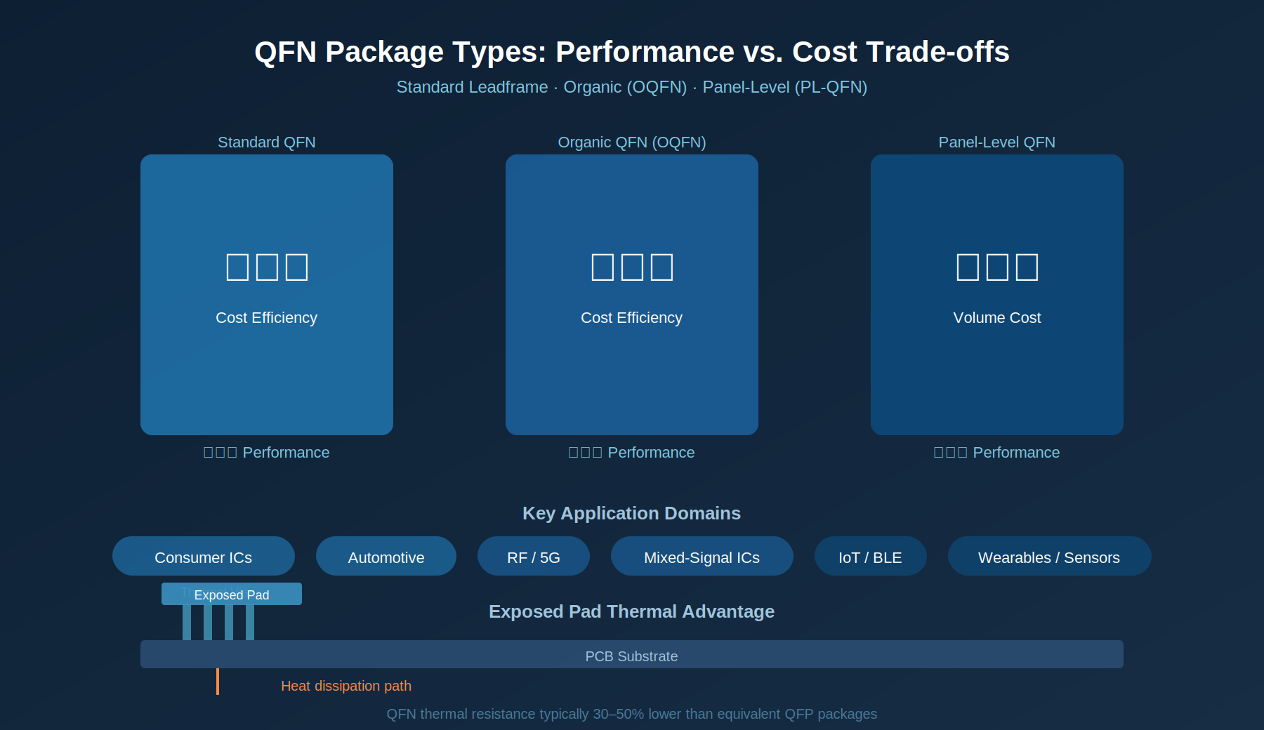
QFN Package Types: A Comparison
While the QFN concept is consistent, several variants have emerged to serve different manufacturing processes and performance requirements:
| Package Variant | Process Basis | Key Advantage | Typical Use |
| Standard QFN | Leadframe + molding | Low cost, mature supply chain | Consumer ICs, PMIC |
| Organic QFN (OQFN) | Organic substrate | Finer pitch, better signal integrity | RF, telecom, mixed-signal |
| Panel-Level QFN (PL-QFN) | Panel-level packaging | Ultra-low cost at volume | IoT, wearables, automotive |
| Dual-Row QFN | Leadframe | Higher I/O density | Connectivity ICs |
| Thermally Enhanced QFN | Leadframe + thermal slug | Superior heat dissipation | Power semiconductors |
Organic QFN: The High-Performance Alternative
Traditional QFN packages use a metal leadframe as the substrate — a cost-effective approach that suits high-volume commodity ICs. Organic QFN replaces the leadframe with an organic laminate substrate, enabling finer pitch routing, better impedance control, and improved electrical performance for RF and mixed-signal applications.
For RF front-end modules, millimeter-wave components, and precision analog ICs, organic QFN delivers performance characteristics that leadframe-based packages cannot match. The substrate enables multi-layer routing, embedded passive integration, and support for tighter pad pitches demanded by advanced silicon nodes.
PCB Technologies’ iNPACK division has developed deep capabilities in organic QFN manufacturing, offering DFM consultation, rapid prototyping, and scalable production. Their approach ensures that performance-optimized designs translate successfully from simulation to silicon.
Panel-Level Packaging: The Cost Revolution
Wafer-level packaging has long been the benchmark for cost-efficient IC packaging in high-volume production — but it is constrained by wafer diameter. Panel-level packaging applies the same lithographic and encapsulation processes to rectangular panels many times larger than a 300mm wafer, dramatically increasing throughput per equipment cycle.
For QFN-type packages produced at scale, panel-level processing can reduce per-unit cost by 30–50% compared to wafer-level equivalents, depending on die size and panel utilization. This cost structure is transforming the economics of IoT components, wireless modules, and automotive sensor ICs — categories where per-unit price pressure is intense.
Thermal Management in QFN Designs
One of the most critical design decisions when using QFN packages is thermal management at the board level. The exposed thermal pad requires careful PCB design to maximize heat transfer:
- Thermal via arrays beneath the exposed pad are strongly recommended for high-power devices
- Pad size should follow IPC-7351 land pattern guidelines for the specific package
- Solder paste aperture design affects both electrical connection and thermal conductivity
- Adjacent ground planes and copper pours help spread heat away from the die
Poor thermal design with QFN packages can negate their inherent thermal advantage, resulting in premature failure or derating. PCB Technologies provides DFM review as part of their packaging engagement, catching thermal design issues before they reach prototype stage.
QFN vs. QFP: When Each Makes Sense
The most common comparison made against QFN is QFP (Quad Flat Package) — the leaded alternative. Each format has its place:
- QFN: Better for high-frequency applications, tighter board area budgets, and superior thermal performance; requires precision solder printing
- QFP: Easier to inspect visually and rework, more forgiving of PCB assembly tolerances; larger footprint
For new designs targeting advanced nodes and compact form factors, QFN consistently wins the performance-per-area tradeoff. The manufacturing challenge of QFN — particularly solder void management under the thermal pad — is well-understood and manageable with proper process controls.
PCB Technologies’ QFN Capability
PCB Technologies offers end-to-end QFN packaging services through their iNPACK platform, spanning design consultation, substrate development, packaging, and test. Their organic QFN capabilities support pitches not achievable with standard leadframe-based processes, making them a strong partner for next-generation wireless, automotive, and medical IC designs.
With established supply chains for organic substrate materials and a track record across demanding qualification standards, PCB Technologies bridges the gap between the cost efficiency demanded by volume production and the performance requirements of advanced applications.
Conclusion
QFN packages continue to evolve — from standard leadframe variants to organic and panel-level formats that unlock new performance and cost tiers. As silicon advances drive smaller die sizes and higher I/O densities, the packaging layer becomes increasingly critical. Selecting the right QFN variant and working with an experienced packaging partner ensures that board-level performance matches the potential of the silicon within.
Electronics
The Rise of System-in-Package (SiP): How Advanced IC Packaging Is Redefining Electronics Miniaturization
As electronics continue to shrink while demands for performance grow, the industry faces a pivotal inflection point. For engineers and product teams researching IC packaging companies capable of delivering complete SiP solutions, understanding the full technology landscape has never been more important.
What Is System-in-Package and Why Does It Matter?
System-in-Package (SiP) is a technology approach that integrates multiple functional components — processors, memory, sensors, RF modules, and passive components — into a single compact package. Unlike a System-on-Chip (SoC), which integrates all functions onto a single die, SiP combines multiple dies and components, often using different process nodes, into one unified module.
This heterogeneous integration approach offers a powerful alternative to traditional multi-chip designs, addressing the core engineering tradeoffs of size, performance, power consumption, and cost. As consumer electronics, wearables, industrial IoT devices, and defense electronics demand ever-smaller form factors without sacrificing functionality, SiP has emerged as a foundational technology for the next generation of electronic systems.
Market Trends Driving SiP Adoption
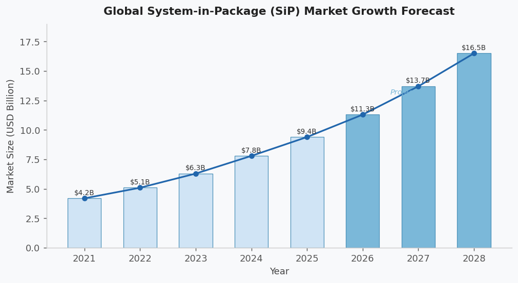
The global SiP market is on a steep growth trajectory. According to industry research, the market was valued at approximately $8 billion in 2024 and is forecast to approach $17 billion by 2028, growing at a compound annual rate exceeding 15%. Several macro trends are powering this expansion:
- IoT and Wearable Devices: The explosion of connected devices demands ultra-compact, low-power modules. SiP allows designers to integrate sensing, processing, and connectivity functions into a package small enough for a smartwatch or medical implant.
- 5G and Advanced Communications: Millimeter-wave 5G systems require highly integrated RF front-end modules. SiP enables the co-packaging of RF components with antenna structures, dramatically reducing signal loss and board real estate.
- Defense and Aerospace Miniaturization: Modern defense electronics — from drone guidance systems to soldier-worn electronics — require extreme miniaturization alongside ultra-high reliability under harsh environmental conditions.
- Medical Device Innovation: Implantable devices, hearing aids, and continuous health monitors are pushing miniaturization to new extremes, where SiP technology enables life-critical functionality in sub-centimeter packages.
- Automotive Electronics: Advanced driver-assistance systems (ADAS) and autonomous vehicle platforms require high-density, thermally reliable SiP modules capable of operating across extreme temperature ranges.
The Technical Challenges of SiP Design and Manufacturing
While SiP offers compelling advantages, its design and manufacturing complexity is substantial. Engineers face a constellation of technical challenges that require deep, cross-domain expertise:
- Thermal Management: Integrating multiple high-power components into a small package concentrates heat significantly. Ensuring reliable thermal dissipation without increasing package height or weight requires sophisticated substrate engineering, embedded coin technology, and careful die placement.
- Signal Integrity and Electromagnetic Interference (EMI): Heterogeneous integration creates complex signal routing challenges. Fine-pitch interconnects between dies must maintain controlled impedance while minimizing crosstalk and EMI — particularly critical in RF and high-speed digital applications.
- CTE Mismatch: Different materials — silicon dies, organic substrates, and passive components — expand and contract at different rates under thermal cycling. Managing coefficient of thermal expansion (CTE) mismatches is essential for long-term reliability, especially in aerospace and defense applications where temperature extremes are the norm.
- Supply Chain Complexity: Traditional SiP development requires coordinating multiple specialized vendors for substrate fabrication, die sourcing, assembly, and testing. Each handoff introduces risk, delay, and potential quality variation.
- Design for Testability: Testing a fully assembled SiP module is fundamentally more difficult than testing individual components. Embedded dies and multi-layer substrates limit physical access, requiring sophisticated In-Circuit Testing (ICT) and system-level test strategies.
The Landscape of SiP Solutions Today
The market has responded to SiP complexity in several ways. Large Outsourced Semiconductor Assembly and Test (OSAT) companies offer high-volume SiP assembly, but their minimum order quantities and standardized processes are often mismatched with the prototype-to-mid-volume needs of defense, aerospace, and medical device companies. Dedicated substrate foundries provide advanced substrate technology but require separate assembly and test partners, fragmenting the supply chain.
The result is that many engineering teams face a frustrating choice: accept the limitations of standardized, high-volume OSAT services, or manage a complex multi-vendor supply chain that introduces quality risk and schedule uncertainty. A third path — working with an integrated, all-in-one solutions provider — is increasingly recognized as the most effective approach for complex, high-reliability SiP programs.
For a deeper understanding of the academic and technical foundations of SiP development, the IEEE Xplore library provides extensive peer-reviewed research on heterogeneous integration, organic substrates, and advanced packaging reliability testing.
How an All-in-One Approach Addresses SiP Complexity
PCB Technologies, with its specialized iNPACK division, has built an integrated capability that directly addresses the core challenges of SiP development. As described on their website, the company is an “All-in-One Solutions Provider of Miniaturization & Advanced IC Packaging Solutions,” operating with a single-roof approach that spans design, substrate fabrication, package assembly, and testing.
Their iNPACK division offers advanced System-in-Package solutions as multi-component, multifunction products. Key capabilities include size reduction, high thermal conductivity, ultra-thin substrates with fine lines and spacing, controlled CTE, 3D design, shielding options, sealing solutions, fine-pitch flip-chip and copper pillar technology, double-side assembly, development and production testing, and full turnkey solutions.
A core differentiator of iNPACK is its organic substrate technology, supporting 25-micron lines and 25-micron spacing — precision that enables the fine-pitch signal routing critical to advanced SiP applications. Their on-site, certified cleanroom manufacturing facility ensures that sensitive components remain free from contamination throughout the assembly process.
Critically, PCB Technologies’ approach eliminates the multi-vendor fragmentation that plagues many SiP programs. Their R&D center is located within the same complex as their manufacturing facilities, enabling seamless transitions from design iteration to prototype production without the handoff delays and communication gaps inherent in fragmented supply chains.
For engineers exploring panel level packaging as an alternative to wafer-level processes, iNPACK’s panel-level approach uses rectangular panels similar to organic substrate manufacturing — designed for efficient production, lower cost per unit, and the flexibility to incorporate Multi-Chip Module (MCM) and SiP assembly on the same production infrastructure.
SiP in Practice: Applications Across High-Demand Industries
The industries best positioned to leverage SiP technology share a common need: maximum functionality in minimum space, with uncompromising reliability. PCB Technologies serves customers across medical, defense, aerospace, communications, and semiconductor sectors — all of which are increasingly turning to SiP as a strategic platform.
- Defense Electronics: Miniaturized radar modules, electronic warfare systems, and soldier-worn communications devices require SiP solutions that maintain performance under shock, vibration, and extreme temperatures. High-reliability SiP with embedded thermal management meets these requirements.
- Medical Devices: From cochlear implants to continuous glucose monitors, medical SiP modules must combine RF, sensing, and processing in biocompatible packages that meet ISO 13485 quality standards — a certification held by PCB Technologies.
- IoT and Industrial Systems: Industrial IoT nodes that operate in harsh environments require rugged SiP modules with wide operating temperature ranges, integrated sensing, and low-power wireless connectivity.
Conclusion: SiP Is No Longer Optional — It Is a Strategic Imperative
System-in-Package technology has moved from a niche solution for space-constrained applications to a mainstream platform technology across multiple high-growth industries. For product teams facing the dual pressure of miniaturization and performance, SiP is increasingly the answer — but only when implemented with the right combination of substrate expertise, assembly precision, and integrated design-to-test capability.
The companies that will lead in the next wave of electronics miniaturization will be those that choose manufacturing partners capable of delivering SiP solutions as an end-to-end, accountable service — from substrate design through final system testing, all under one roof.
Electronics
AI Modules and Smart Home Chips: Future of Home Automation
Welcome to a world where your home is not just smart, but intelligent. Imagine walking into a room that anticipates your needs before you even utter a word. Picture a house that adapts seamlessly to your lifestyle, making everyday tasks effortless and efficient. This is the future of home automation, powered by AI modules and smart home chips. In this blog post, we will dive deep into the realm of artificial intelligence (AI) and explore how these innovative technologies are reshaping the way we live in our homes. Get ready to embark on an extraordinary journey where science fiction becomes reality – welcome to the future of home automation!
The concept of a “smart home” has transformed from a futuristic fantasy into a reality in recent years. Thanks to advancements in technology, particularly in the fields of AI (Artificial Intelligence) and IoT (Internet of Things), homes can now be equipped with devices and systems that offer convenience, energy efficiency, and enhanced security. Key components driving this transformation are AI modules and smart home chips, which serve as the brains behind smart devices and enable them to communicate, process data, and make intelligent decisions. In this article, we will delve into the world of AI modules and smart home chips, exploring their functions, applications, and the impact they have on shaping the future of home automation.
AI Modules: The Brains Behind Smart Homes
AI modules are compact computing devices that integrate specialized hardware and software to perform AI-related tasks. These modules are designed to process data, recognize patterns, and make decisions, all with the goal of adding intelligence to everyday devices within a smart home ecosystem. The power of AI modules lies in their ability to analyze vast amounts of data quickly and efficiently, enabling smart devices to adapt to user preferences and changing conditions.
Key Functions of AI Modules in Smart Homes:
- Voice Recognition and Control: AI modules often include voice recognition capabilities, allowing users to control smart devices through voice commands. Whether it’s adjusting the thermostat, playing music, or dimming the lights, voice control simplifies daily tasks.
- Predictive Analysis: AI modules can analyze historical data and user behavior to make predictions about future preferences and needs. For example, they can learn when residents are likely to be home and adjust heating or cooling accordingly.
- Security and Surveillance: AI modules enhance home security by analyzing camera feeds and alerting homeowners to potential threats or unusual activities. They can distinguish between ordinary events and suspicious ones, reducing false alarms.
- Energy Management: These modules optimize energy usage by monitoring energy consumption patterns and suggesting ways to reduce waste. For instance, they can turn off lights and appliances when not in use or adjust heating and cooling based on occupancy.
- Personalization: AI modules tailor smart home experiences to individual preferences. They learn user habits and adjust settings for lighting, temperature, and entertainment accordingly.
Smart Home Chips: Enabling Connectivity and Efficiency
Smart home chips, also known as microcontrollers or system-on-chip (SoC) solutions, are the hardware components that enable devices to connect to each other and the internet, forming a cohesive smart home network. These chips are the foundation of IoT devices, allowing them to communicate, receive updates, and function seamlessly within a smart home ecosystem. Smart home chips come in various forms and offer different communication protocols, catering to the diverse needs of smart devices.

Key Functions of Smart Home Chips in Smart Homes:
- Connectivity: Smart home chips provide the necessary wireless connectivity, such as Wi-Fi, Bluetooth, Zigbee, or Z-Wave, for devices to communicate with each other and with the homeowner’s smartphone or central hub.
- Data Processing: These chips handle data processing tasks, including sensor data interpretation, encryption for security, and communication with cloud-based services for remote control and monitoring.
- Low Power Consumption: To ensure the longevity of battery-powered devices, smart home chips are designed for energy efficiency. They optimize power usage to extend battery life.
- Interoperability: Smart home chips adhere to industry standards and communication protocols, ensuring that devices from different manufacturers can work together seamlessly in a connected home environment.
Applications of AI Modules and Smart Home Chips
The combined power of AI modules and smart home chips opens up a wide range of applications within smart homes:
- Smart Lighting: AI modules can adjust lighting based on natural light, time of day, and user preferences, while smart home chips enable remote control and scheduling of lights.
- Climate Control: AI modules optimize heating and cooling systems, while smart home chips allow users to adjust temperatures remotely or based on occupancy.
- Security and Surveillance: AI modules analyze camera feeds for security threats, while smart home chips enable real-time monitoring and alerts.
- Voice Assistants: AI modules power voice-activated assistants like Amazon Alexa and Google Assistant, while smart home chips facilitate communication between these devices and other smart appliances.
- Energy Management: AI modules monitor energy consumption patterns, while smart home chips provide the connectivity for users to remotely control and adjust devices for energy efficiency.
- Appliance Automation: AI modules can learn user habits and preferences, allowing for automatic control of appliances like washing machines, ovens, and refrigerators.
- Health and Wellbeing: AI modules can monitor health-related data, such as sleep patterns or air quality, while smart home chips enable data transmission to healthcare providers or family members.
The Future of Smart Homes with AI Modules and Smart Home Chips
The future of smart homes is filled with promise, as AI modules and smart home chips continue to advance. Here are some trends to watch for:
- Increased Integration: AI modules will become more integrated into everyday objects and devices, making them smarter and more intuitive to use.
- Enhanced Security: Smart home chips will feature improved security measures to protect user data and privacy, addressing concerns about cybersecurity.
- Energy Efficiency: AI modules will play a crucial role in further optimizing energy usage, reducing environmental impact, and lowering utility costs.
- Voice and Gesture Recognition: AI modules will continue to improve voice and gesture recognition, making human-computer interaction even more natural and intuitive.
- Health and Wellness: AI modules will take on a larger role in monitoring and promoting health and wellness within the smart home environment.
Conclusion
AI modules and smart home chips are the driving force behind the modern smart home revolution. They provide the intelligence and connectivity needed to create a seamless and efficient living environment that enhances convenience, security, and energy efficiency. As these technologies continue to advance, we can expect smarter, more connected, and more personalized homes that cater to our evolving needs and preferences. The future of home automation is indeed bright, thanks to AI modules and smart home chips.
FAQs
- What is the role of AI modules in a smart home?
- AI modules serve as the intelligence behind smart home devices. They analyze data, recognize patterns, and make decisions to enhance convenience, security, and energy efficiency within a smart home ecosystem.
- How do AI modules enhance voice control in smart homes?
- AI modules enable voice recognition and control, allowing users to interact with smart devices using voice commands. This feature simplifies tasks like adjusting lighting, thermostats, and entertainment systems.
- What functions do smart home chips perform in a smart home environment?
- Smart home chips provide connectivity for devices, enabling them to communicate with each other and with central hubs or smartphones. They handle data processing, optimize power consumption, and ensure interoperability among devices.
- How do smart home chips contribute to energy efficiency in smart homes?
- Smart home chips optimize energy usage by facilitating the remote control and scheduling of devices. They ensure that devices consume power efficiently and can even help reduce energy waste.
- Can AI modules and smart home chips work together to enhance smart home features?
- Yes, AI modules and smart home chips often collaborate to create smart home features. For example, AI modules analyze sensor data, and smart home chips enable communication and control of devices based on AI module insights.
- Are smart home chips secure, considering the rise in concerns about cybersecurity?
- Manufacturers of smart home chips are increasingly prioritizing security. They implement measures to protect user data and privacy, and advancements in security protocols are continually enhancing chip security.
- What is the future outlook for smart homes with AI modules and smart home chips?
- The future of smart homes holds promise with increased integration, enhanced security, improved energy efficiency, and more intuitive voice and gesture recognition. These technologies will continue to advance, creating smarter, healthier, and more connected living spaces.

Targeted Vertical Incubation: Strategic Alignment in Technical Software Venture Co-Investments

The Critical Technical SEO Audit Checklist for Enterprise SaaS Environments

Shadow AI Detection: Regaining Visibility Over Unsanctioned Enterprise Tooling

-

 Business Solutions2 years ago
Live Video Broadcasting with Bonded Transmission Technology
-

 Business Solutions1 year ago
The Future of Healthcare SMS and RCS Messaging
-

 Business Solutions2 years ago
2-Way Texting Solutions from Company Message Services
-

 Business Solutions2 years ago
Communication with Analog to Fiber Converters & RF Link Budgets
-

 DSRC Communication1 year ago
The Crossroads of Connectivity: DSRC vs. C-V2X Technologies in Automotive Communication
-
Electronics3 years ago
AI Modules and Smart Home Chips: Future of Home Automation
-

 Business Solutions2 years ago
Wholesale SMS Platforms with OTP Services
-

 Business Solutions1 year ago
Choosing the Right B2B Digital Marketing Agency: A Guide