Automotive
Wire Bonding vs. Flip Chip: Navigating the Evolving World of IC Interconnect Technology
Summary: IC interconnect technology – how a semiconductor die connects electrically to its substrate or package – is one of the most consequential decisions in modern electronics design.
This article examines: the technical fundamentals of wire bonding and flip chip packaging; the market trends reshaping interconnect technology choices; the engineering tradeoffs that determine which approach is optimal for a given application; the landscape of available solutions; and how an integrated packaging capability enables engineers to access both technologies – and choose freely between them – within a single supply chain.
For engineers evaluating interconnect strategies for their next design, understanding the full depth of wire bonding options and their flip chip alternatives is essential. The choice directly affects device performance, package size, signal integrity, manufacturing cost, and qualification timeline.
The Fundamentals: What Wire Bonding and Flip Chip Actually Are
At its core, the IC interconnect challenge is straightforward: a semiconductor die contains hundreds or thousands of tiny electrical contact pads. Those pads must be connected to the package substrate – which then connects to the PCB – with minimal resistance, inductance, and crosstalk, while maintaining mechanical integrity through thermal cycling, vibration, and shock.
Wire Bonding is the oldest and most widely used interconnect technique. Thin wires – typically gold, copper, or aluminum – are bonded from the die bond pads to the package substrate using thermal compression, ultrasonic energy, or a combination of both (thermosonic bonding). The resulting wire loops are visible under a microscope as delicate arcs spanning from die to substrate.
Flip Chip packaging inverts this approach. Instead of bonding wires from the top surface of the die, the die is flipped face-down, with solder bumps or copper pillars on the active surface connecting directly to matching pads on the substrate. The entire connection is made through these bumps in a single reflow step, with no wire loops.
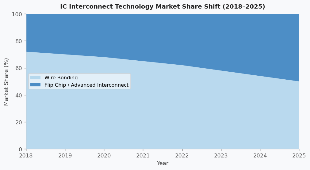

Market Trends: The Steady Rise of Flip Chip
The global IC packaging market is undergoing a structural shift away from wire bonding as the dominant interconnect approach, driven by the performance demands of advanced applications. Industry research indicates that flip chip packaging now accounts for roughly half of the total IC interconnect market by value, with penetration continuing to grow in high-performance segments.
Several converging trends are driving this shift:
- High-Speed Digital Performance: Modern processors, memory controllers, and network chips operate at speeds where wire inductance – an inherent characteristic of wire bond loops – causes signal integrity problems. Flip chip’s shorter, lower-inductance interconnects are essential for chips operating above a few gigahertz.
- Fine-Pitch I/O Requirements: As die complexity increases, the number of I/O connections grows and their pitch shrinks. Advanced chips now require hundreds to thousands of I/O connections at pitches that wire bonding cannot reliably achieve, but flip chip copper pillars can support.
- Thermal Performance: Flip chip’s inverted die placement exposes the back side of the silicon directly upward, enabling direct attachment of a heatsink to the die – dramatically improving thermal dissipation compared to wire bonded packages where the die back faces the substrate.
- Package Height Reduction: Wire bond loops require vertical clearance above the die. Flip chip eliminates this requirement, enabling ultra-thin packages critical for wearables, implantable medical devices, and ultra-thin consumer electronics.
Where Wire Bonding Remains the Optimal Choice
Despite the growth of flip chip, wire bonding is far from obsolete – and for many applications, it remains the technically and economically optimal choice.
- Cost-Sensitive, Standard I/O Applications: Wire bonding equipment and processes are mature, widely available, and highly cost-effective for chips with moderate I/O counts and standard pitch. For commodity sensors, microcontrollers, and discrete semiconductors, wire bonding delivers excellent performance at minimal cost.
- Mixed-Die Assemblies: In multi-chip module (MCM) designs and System-in-Package (SiP) assemblies, wire bonding enables flexible interconnection between dies of different sizes and heights – including die-to-die connections within the same package that would be impractical with bump-based approaches.
- Known-Good Die (KGD) Management: Wire bonding can be performed after functional testing of individual dies, reducing the risk of assembling expensive SiP modules with defective components.
- Rework Capability: Wire bonds can be selectively reworked – broken bonds can be re-bonded – providing a repair option that flip chip assemblies generally do not offer, which is valuable in low-volume, high-value applications.
Flip Chip vs. Wire Bond: The Engineering Decision Framework
The choice between flip chip vs wire bond is not a binary decision with a universal right answer. It is a multi-dimensional optimization across performance, cost, form factor, reliability, and supply chain complexity. The key decision drivers include:
- Operating Frequency: For applications below approximately 1 GHz, wire bonding is typically sufficient. For RF, mmWave, and high-speed digital applications above a few GHz, flip chip’s lower parasitics become essential.
- I/O Count and Pitch: For designs with more than a few hundred I/O at fine pitch, flip chip or copper pillar technology is generally required. Wire bonding becomes physically impractical at very high I/O densities.
- Package Thickness: For applications where vertical space is at a premium, flip chip eliminates the wire loop height overhead – typically 200–400 microns – enabling thinner packages.
- Thermal Requirements: High-power dies benefit significantly from the superior thermal path provided by direct heatsink attachment enabled by flip chip orientation.
- Volume and Cost Sensitivity: At low-to-medium volumes, wire bonding is typically more cost-effective. At high volumes, the economics become more application-specific and are influenced heavily by substrate cost, yield, and test strategy.
The Integration Advantage: Access to Both Technologies in One Supply Chain
One of the most underappreciated challenges in advanced IC packaging is the supply chain fragmentation that results when different interconnect technologies require different vendors. Many organizations source wire bonding from one assembly house, flip chip from another, and organic substrates from a third – creating a coordination burden that adds time, cost, and quality risk to every program.
PCB Technologies, through its iNPACK division, offers a fundamentally different model. As described in their materials, the iNPACK division provides complete package PCB assembly solutions including SiP design and manufacturing, surface mount technology, chip on board (COB) wire bonding, microfabrication, and substrate design and manufacturing – all under one roof.
Their substrate technology supports 25-micron lines and 25-micron spacing, enabling the fine-pitch routing required for both advanced wire bond fan-out designs and flip chip copper pillar interconnects. Their cleanroom manufacturing facility, certified to ISO 9001, ISO 14001, ISO 13485, and AS 9100, ensures the contamination control and process discipline required for reliable advanced interconnects.
For engineers seeking academic grounding in IC interconnect technologies, IEEE Xplore provides extensive peer-reviewed literature on wire bonding reliability, flip chip process development, and advanced packaging interconnect performance – an essential reference for teams evaluating interconnect technology choices.
The Path Forward: Heterogeneous Integration
The most sophisticated packaging programs today do not choose between wire bonding and flip chip – they use both, strategically, within the same SiP module. A high-power processor might use copper pillar flip chip interconnects for maximum performance, while peripheral functions such as a power management IC, a sensor die, or an RF module are wire bonded to the same substrate.
This heterogeneous integration approach requires the substrate to accommodate both interconnect types simultaneously, with the DfM expertise to ensure that both are manufacturable, testable, and reliable at production scale. It is a capability that demands deep, integrated expertise across substrate design, interconnect technology, assembly process, and test engineering.
Conclusion: The Right Interconnect for the Right Application
Wire bonding and flip chip packaging represent complementary – not competing – technologies in the modern IC packaging toolkit. The engineering challenge is not to choose one universally, but to understand each application’s specific requirements deeply enough to select the right approach, and to partner with a manufacturing organization capable of executing either strategy with equal precision and accountability.
As miniaturization continues to advance and new application categories – implantable medical devices, next-generation defense electronics, advanced automotive systems – push the boundaries of what is possible, the ability to access both interconnect technologies through a single, integrated supply chain will increasingly determine which organizations can deliver on their design intent.