Industrial Solutions
System in Package vs. SoC vs. MCM: Choosing the Right Integration Approach

Key Takeaways
- A system in package (SiP) integrates separately manufactured dies, passives, MEMS and RF components into one package that performs a complete system function.
- Unlike a system-on-chip, a SiP can combine dies built on different processes and materials, such as silicon CMOS, SiGe, GaAs and GaN.
- A multi-chip module typically forms a tightly coupled subsystem, while a SiP is usually expected to deliver a complete system.
- SiP improves yield because a die that fails inspection can be replaced before assembly instead of scrapping the whole system.
Engineers comparing integration options usually end up weighing three approaches: put everything on one die, place several dies on a shared substrate, or build a complete subsystem inside a single package. Those choices go by the names system-on-chip (SoC), multi-chip module (MCM) and system-in-package (SiP), and the differences between them shape cost, yield, schedule and how much freedom a design team has to mix technologies. This guide compares the three side by side and explains where each one fits.
What is a system in package (SiP)?
A system in package is a single package that integrates multiple separately manufactured components, such as dies, passives, MEMS devices and RF parts, into one assembly that performs a complete system function. The IEEE Heterogeneous Integration Roadmap uses almost exactly this framing, describing heterogeneous integration as combining separately manufactured components into a higher-level assembly, the SiP, that delivers enhanced functionality and improved operating characteristics. In that definition, a component can be an individual die, a MEMS device, a passive component, or an already assembled package or subsystem.
A useful practical description of system in package technology frames the goal as a system close to the SoC form factor, but with better yield, lower overall cost, higher flexibility and a faster route to market. SiP designs draw on a growing toolbox: vertical and horizontal interconnect technologies, encapsulation for protection and stabilization, and a wide range of packaging architectures.
How is a SiP different from a system-on-chip?
A system-on-chip builds all functions into one monolithic piece of silicon on a single process node, while a SiP assembles several dies, each potentially made on a different process and material, inside one package. That distinction matters because logic, RF, power and sensing functions rarely perform best on the same process. The IEEE overview of SiP technology notes that heterogeneous integration lets a package combine dies built in different process nodes and materials, including silicon CMOS, SiGe, GaAs and GaN. An SoC cannot do that by definition.
Yield is the second major difference. With a monolithic die, a defect anywhere can scrap the whole chip. In a SiP, a die that fails incoming inspection can be replaced before assembly without discarding the rest of the system, which is one reason SiP is often described as the higher-yield path to SoC-like density.
How is a SiP different from a multi-chip module?
A multi-chip module places two or more dies on a shared substrate so they operate as one tightly coupled component, whereas a SiP is usually expected to deliver a complete system function. The two terms overlap heavily, and many engineers use them loosely, but the difference lies mainly in scope. An MCM typically represents a tightly coupled subsystem, such as a processor paired with memory, rather than a whole system. A SiP more often pulls in passives, filters, sensors or MEMS alongside the dies, so the finished part can act as a self-contained functional block.
Historically, the biggest obstacle for both approaches was the availability of known good die (KGD): if bare dies cannot be fully tested before assembly, the yield advantage of multi-die integration shrinks quickly. Improvements in die-level testing are a large part of why multi-die packaging has become mainstream.

SiP vs. SoC vs. MCM: how do they compare?
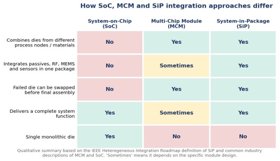
The quickest way to compare the three approaches is by what each one integrates, how it handles yield, and where it typically shows up in products. The table below summarizes the main differences.
| Factor | System-on-Chip (SoC) | Multi-Chip Module (MCM) | System-in-Package (SiP) |
| What is integrated | All functions on one monolithic die | Two or more dies on a shared substrate | Dies plus passives, RF, MEMS or sensors in one package |
| Mixed process nodes and materials | No | Yes | Yes |
| Yield behavior | One defect can scrap the whole die | Depends on known good die | Failed die can be replaced before assembly |
| Typical scope | Complete system on silicon | Tightly coupled subsystem | Complete system function |
| Main trade-off | High development cost and long design cycles | Substrate, thermal and test complexity | Package co-design and test complexity |
Why is testing a SiP harder than testing a single chip?
Testing a SiP is harder because a single package contains several different kinds of devices, and digital, analog and RF dies each need their own test approach. For digital dies, the IEEE 1149.1 boundary-scan standard and its extensions provide structured test access. Analog and RF components are a different story: they still require custom test strategies and probe access at the package pins. That makes reliability engineering a central part of any SiP program, not an afterthought. A detailed look at SiP reliability analysis and test methods shows how failure analysis and qualification testing fit into the development cycle.
Which manufacturing routes are used to build SiPs?
SiPs can be built on organic laminate substrates, on wafer-level redistribution layers, or on large rectangular panels, and the right route depends on volume, feature size and cost targets. Wafer-level approaches use redistribution, fan-out or stacking processes to connect multiple dies before the package is completed. Panel-based processing applies similar ideas to a larger format, and engineers weighing the two can compare panel-level versus wafer-level processing to understand where each makes economic sense.
Where horizontal space runs out, designers move vertically. Package-on-package (PoP), common in mobile processors, stacks a memory package on top of a logic package and connects them at the package boundary, reaching high memory bandwidth without a dedicated interposer. More advanced options place dies side by side on an interposer or stack them directly, and an overview of 2.5D and 3D die stacking options covers how those architectures change routing, thermal and assembly requirements.
Which industries are driving SiP adoption?
High-performance computing, mobile devices, automotive, medical wearables, aerospace and defense, and IoT are the main markets pushing SiP and heterogeneous integration forward. Those six application areas are named as the leading drivers in the Heterogeneous Integration Roadmap, which has been sponsored since 2015 by the IEEE Electronics Packaging Society, SEMI, the IEEE Electron Devices Society, the IEEE Photonics Society and the ASME EPPD Division, after the Semiconductor Industry Association closed the earlier ITRS roadmap. The roadmap’s public program page on SEMI’s site explains how the effort is governed, and the 2025 edition updated 25 chapters. Across all of these markets, the appeal is the same: SoC-like density without forcing every function onto one process.
When should a design team choose SiP over SoC or MCM?
SiP is usually the better choice when a product needs functions built on different semiconductor processes, when volumes do not justify a custom SoC, or when the schedule cannot absorb a full silicon development cycle. An SoC still makes sense for very high-volume products where the up-front development cost can be spread across millions of units and every square millimeter and milliwatt counts. An MCM fits well when the goal is a tightly coupled pair or group of dies, such as compute with memory, rather than a complete system.
For many programs, the decision comes down to three questions. Do the required functions share a process node? Is the volume high enough to amortize custom silicon? And is the team prepared to co-design the die, package and board together? If the honest answers are no, no and yes, a SiP is very likely the right fit. The IEEE topic overview of system-in-package is a good neutral starting point for teams new to the trade-offs.
Frequently Asked Questions
What is the difference between SiP and SoC?
A system-on-chip puts all functions on one monolithic die built on a single process, while a system in package combines several separately manufactured dies and components, often from different processes and materials, inside one package.
Is a multi-chip module the same as a system in package?
Not exactly. A multi-chip module usually describes several dies on a shared substrate acting as a tightly coupled subsystem, while a system in package is generally expected to deliver a complete system function and often includes passives, RF parts, sensors or MEMS.
Why do system in package designs often have better yield than SoCs?
In a system in package, a die that fails inspection can be replaced before assembly, so one defect does not scrap the entire system the way it can with a single monolithic die.
Which industries use system in package technology?
System in package technology is widely used in high-performance computing, mobile devices, automotive electronics, medical wearables, aerospace and defense, and IoT products.