Automotive
The Rise of System-in-Package (SiP): How Advanced IC Packaging Is Redefining Electronics Miniaturization
Summary: System-in-Package (SiP) technology is one of the fastest-growing segments in semiconductor packaging, driven by demand for compact, high-performance devices across healthcare, defense, aerospace, and consumer electronics.
This article covers: what SiP is and why it matters; key market trends and drivers; the technical challenges facing engineers; the landscape of existing solutions; and how an all-in-one manufacturing approach delivers a competitive edge in SiP design and production.
As electronics continue to shrink while demands for performance grow, the industry faces a pivotal inflection point. For engineers and product teams researching IC packaging companies capable of delivering complete SiP solutions, understanding the full technology landscape has never been more important.
What Is System-in-Package and Why Does It Matter?
System-in-Package (SiP) is a technology approach that integrates multiple functional components – processors, memory, sensors, RF modules, and passive components – into a single compact package. Unlike a System-on-Chip (SoC), which integrates all functions onto a single die, SiP combines multiple dies and components, often using different process nodes, into one unified module.
This heterogeneous integration approach offers a powerful alternative to traditional multi-chip designs, addressing the core engineering tradeoffs of size, performance, power consumption, and cost. As consumer electronics, wearables, industrial IoT devices, and defense electronics demand ever-smaller form factors without sacrificing functionality, SiP has emerged as a foundational technology for the next generation of electronic systems.
Market Trends Driving SiP Adoption
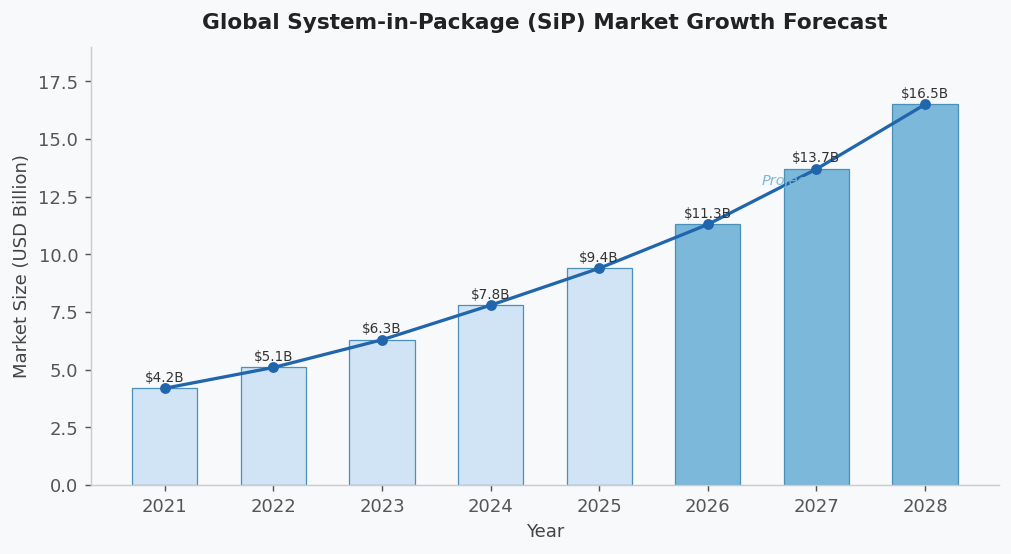
The global SiP market is on a steep growth trajectory. According to industry research, the market was valued at approximately $8 billion in 2024 and is forecast to approach $17 billion by 2028, growing at a compound annual rate exceeding 15%. Several macro trends are powering this expansion:
- IoT and Wearable Devices: The explosion of connected devices demands ultra-compact, low-power modules. SiP allows designers to integrate sensing, processing, and connectivity functions into a package small enough for a smartwatch or medical implant.
- 5G and Advanced Communications: Millimeter-wave 5G systems require highly integrated RF front-end modules. SiP enables the co-packaging of RF components with antenna structures, dramatically reducing signal loss and board real estate.
- Defense and Aerospace Miniaturization: Modern defense electronics – from drone guidance systems to soldier-worn electronics – require extreme miniaturization alongside ultra-high reliability under harsh environmental conditions.
- Medical Device Innovation: Implantable devices, hearing aids, and continuous health monitors are pushing miniaturization to new extremes, where SiP technology enables life-critical functionality in sub-centimeter packages.
- Automotive Electronics: Advanced driver-assistance systems (ADAS) and autonomous vehicle platforms require high-density, thermally reliable SiP modules capable of operating across extreme temperature ranges.

The Technical Challenges of SiP Design and Manufacturing
While SiP offers compelling advantages, its design and manufacturing complexity is substantial. Engineers face a constellation of technical challenges that require deep, cross-domain expertise:
- Thermal Management: Integrating multiple high-power components into a small package concentrates heat significantly. Ensuring reliable thermal dissipation without increasing package height or weight requires sophisticated substrate engineering, embedded coin technology, and careful die placement.
- Signal Integrity and Electromagnetic Interference (EMI): Heterogeneous integration creates complex signal routing challenges. Fine-pitch interconnects between dies must maintain controlled impedance while minimizing crosstalk and EMI – particularly critical in RF and high-speed digital applications.
- CTE Mismatch: Different materials – silicon dies, organic substrates, and passive components – expand and contract at different rates under thermal cycling. Managing coefficient of thermal expansion (CTE) mismatches is essential for long-term reliability, especially in aerospace and defense applications where temperature extremes are the norm.
- Supply Chain Complexity: Traditional SiP development requires coordinating multiple specialized vendors for substrate fabrication, die sourcing, assembly, and testing. Each handoff introduces risk, delay, and potential quality variation.
- Design for Testability: Testing a fully assembled SiP module is fundamentally more difficult than testing individual components. Embedded dies and multi-layer substrates limit physical access, requiring sophisticated In-Circuit Testing (ICT) and system-level test strategies.
The Landscape of SiP Solutions Today
The market has responded to SiP complexity in several ways. Large Outsourced Semiconductor Assembly and Test (OSAT) companies offer high-volume SiP assembly, but their minimum order quantities and standardized processes are often mismatched with the prototype-to-mid-volume needs of defense, aerospace, and medical device companies. Dedicated substrate foundries provide advanced substrate technology but require separate assembly and test partners, fragmenting the supply chain.
The result is that many engineering teams face a frustrating choice: accept the limitations of standardized, high-volume OSAT services, or manage a complex multi-vendor supply chain that introduces quality risk and schedule uncertainty. A third path – working with an integrated, all-in-one solutions provider – is increasingly recognized as the most effective approach for complex, high-reliability SiP programs.
For a deeper understanding of the academic and technical foundations of SiP development, the IEEE Xplore library provides extensive peer-reviewed research on heterogeneous integration, organic substrates, and advanced packaging reliability testing.
How an All-in-One Approach Addresses SiP Complexity
PCB Technologies, with its specialized iNPACK division, has built an integrated capability that directly addresses the core challenges of SiP development. As described on their website, the company is an “All-in-One Solutions Provider of Miniaturization & Advanced IC Packaging Solutions,” operating with a single-roof approach that spans design, substrate fabrication, package assembly, and testing.
Their iNPACK division offers advanced System-in-Package solutions as multi-component, multifunction products. Key capabilities include size reduction, high thermal conductivity, ultra-thin substrates with fine lines and spacing, controlled CTE, 3D design, shielding options, sealing solutions, fine-pitch flip-chip and copper pillar technology, double-side assembly, development and production testing, and full turnkey solutions.
A core differentiator of iNPACK is its organic substrate technology, supporting 25-micron lines and 25-micron spacing – precision that enables the fine-pitch signal routing critical to advanced SiP applications. Their on-site, certified cleanroom manufacturing facility ensures that sensitive components remain free from contamination throughout the assembly process.
Critically, PCB Technologies’ approach eliminates the multi-vendor fragmentation that plagues many SiP programs. Their R&D center is located within the same complex as their manufacturing facilities, enabling seamless transitions from design iteration to prototype production without the handoff delays and communication gaps inherent in fragmented supply chains.
For engineers exploring panel level packaging as an alternative to wafer-level processes, iNPACK’s panel-level approach uses rectangular panels similar to organic substrate manufacturing – designed for efficient production, lower cost per unit, and the flexibility to incorporate Multi-Chip Module (MCM) and SiP assembly on the same production infrastructure.
SiP in Practice: Applications Across High-Demand Industries
The industries best positioned to leverage SiP technology share a common need: maximum functionality in minimum space, with uncompromising reliability. PCB Technologies serves customers across medical, defense, aerospace, communications, and semiconductor sectors – all of which are increasingly turning to SiP as a strategic platform.
- Defense Electronics: Miniaturized radar modules, electronic warfare systems, and soldier-worn communications devices require SiP solutions that maintain performance under shock, vibration, and extreme temperatures. High-reliability SiP with embedded thermal management meets these requirements.
- Medical Devices: From cochlear implants to continuous glucose monitors, medical SiP modules must combine RF, sensing, and processing in biocompatible packages that meet ISO 13485 quality standards – a certification held by PCB Technologies.
- IoT and Industrial Systems: Industrial IoT nodes that operate in harsh environments require rugged SiP modules with wide operating temperature ranges, integrated sensing, and low-power wireless connectivity.
Conclusion: SiP Is No Longer Optional — It Is a Strategic Imperative
System-in-Package technology has moved from a niche solution for space-constrained applications to a mainstream platform technology across multiple high-growth industries. For product teams facing the dual pressure of miniaturization and performance, SiP is increasingly the answer – but only when implemented with the right combination of substrate expertise, assembly precision, and integrated design-to-test capability.
The companies that will lead in the next wave of electronics miniaturization will be those that choose manufacturing partners capable of delivering SiP solutions as an end-to-end, accountable service – from substrate design through final system testing, all under one roof.