Tech
PCB Board Manufacturer: What PCB Manufacturing and Fabrication Actually Involve

Key Takeaways
|
What does a PCB board manufacturer actually do, start to finish?
The scope of what a PCB board manufacturer offers varies considerably between suppliers, and that scope has real consequences for how a project actually gets executed. PCB Technologies’ own description of its manufacturing scope is instructive here: an all-in-one solutions provider covering high-mix multilayer rigid, rigid-flex, and multi-flex PCBs, substrates, IC packaging, complex electronic component assemblies, and electro-mechanical sub-systems, supplying everything from bare board manufacturing to finished electronic products. A manufacturer with that full-process, in-house scope can carry a design from a quick-turn prototype through cost-effective mid-to-high-volume production without handing the project off between multiple vendors along the way.
What do the basic PCB manufacturing terms actually mean?
PCB manufacturing has its own specific vocabulary, and understanding these terms precisely matters when specifying a board or reviewing a quote, since each one describes a measurable characteristic that affects performance and cost.
| Term | What it actually means |
|---|---|
| Copper weight | An indicator of copper foil thickness on each PCB layer, typically expressed in ounces of copper per square foot. |
| FR4 | The most commonly used PCB substrate material, a flame-resistant fiberglass-reinforced epoxy laminate. |
| Multi-layer PCB | A PCB with at least three conductive layers of traces and components, as opposed to single or double-sided boards. |
| HDI (High-Density Interconnect) | Advanced PCB fabrication technology using micro blind vias to create boards with high trace density. |
Other foundational terms round out the basics: a Gerber file is the standard file format used to communicate board specifications to manufacturers for controlling photoplotters, and a pad is a contact point used to connect components with vias, where components are ultimately soldered. Getting these specifications wrong, or leaving them ambiguous, is a common source of costly miscommunication between a designer and a manufacturer.
How does PCB fabrication actually differ from PCB assembly?
It’s easy to use “PCB manufacturing” as a catch-all term, but fabrication and assembly are genuinely distinct stages of production. PCB fabrication is the process of actually building the bare board itself, layering copper and substrate material, drilling and plating vias, and etching the copper into the circuit pattern the design calls for. PCB assembly, sometimes abbreviated PCBA, comes after fabrication: it’s the process of populating that finished bare board with electronic components and soldering them into place. A PCB board manufacturer offering both stages in-house removes a hand-off point between two separate vendors, which can otherwise introduce delays, miscommunication, or quality inconsistency between the bare board and its final assembled state.
Why does the choice between subtractive processing and mSAP actually matter?
Not every PCB fabrication process is interchangeable, and the choice between them has real implications for what a board can actually achieve. PCB Technologies’ comparison of subtractive processing and mSAP lays out the distinction clearly: subtractive photolithography is a well-established method of producing high-quality PCBs and microelectronics, considered the industry standard and applicable across a wide range of designs, from simple single-layer boards to complex multilayer ones. Modified semi-additive processing (mSAP), meanwhile, is particularly well suited to manufacturing High-Density Interconnect (HDI) boards, since it facilitates the kind of intricate circuitry HDI designs require to incorporate multiple layers of copper traces and vias within very tight spaces.
How large is the global demand this industry serves?
PCB manufacturing sits underneath nearly every category of modern electronics, which shows up clearly in the scale of the underlying market. IMARC Group’s printed circuit board market analysis values the global market at $70.7 billion in 2023, projected to reach $97.6 billion by 2032, a compound annual growth rate of 3.4%. That steady, broad-based growth reflects the PCB’s role as foundational infrastructure across computing, communications, automotive, medical, and defense electronics alike, rather than a category driven by any single dominant end use.
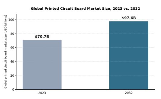

Global printed circuit board market size, 2023 versus 2032, according to IMARC Group.
What industries actually depend on advanced PCB manufacturing and fabrication capability?
- Military and defense: mission-critical PCBs designed to operate reliably under extreme environmental conditions.
- Aerospace: high-reliability boards where failure is not an acceptable outcome given the operating environment.
- Medical: boards subject to strict regulatory and reliability requirements, often for life-critical devices.
- RF/microwave and robotics/automation: applications demanding specialized materials and precise signal integrity performance.
What should you actually evaluate when choosing a PCB board manufacturer?
Beyond price and lead time, the more consequential questions concern process scope and in-house capability. Does the manufacturer handle both fabrication and assembly in-house, or does the board change hands between separate vendors partway through production? Can the same manufacturer support both quick-turn prototypes and higher-volume production runs without switching processes or facilities entirely? And does their process lineup include the specific techniques, like mSAP for HDI designs, that a given board’s complexity actually requires? Answering these questions upfront avoids discovering a capability gap midway through a project, when switching manufacturers becomes far more costly than it would have been at the outset.
Why does certification coverage matter as much as manufacturing capability?
A PCB board manufacturer’s technical capability only matters if it’s backed by certifications relevant to the industry the finished board will actually serve. Military and defense electronics typically require certifications like AS9100 and various MIL specifications; medical devices demand ISO 13485 compliance; and automotive electronics increasingly require IATF 16949 alongside general quality standards like ISO 9001. A manufacturer’s certification portfolio isn’t just paperwork; it reflects whether their quality management systems, documentation practices, and traceability processes have actually been audited against the standards a regulated industry requires. Checking certification coverage against a project’s actual end market, rather than assuming general PCB competence is sufficient, avoids a costly late-stage discovery that a manufacturer can’t support the compliance documentation a customer or regulator ultimately requires.
What does a typical PCB manufacturing workflow actually look like end to end?
Understanding the sequence of steps a board actually passes through helps explain why certain design decisions early on affect cost and timeline so significantly later. Manufacturing begins with the inner and outer layer materials being cut to the required dimensions, a step known as blanking, before those layers are cleaned, treated, and imaged with the circuit pattern using a photosensitive dry film exposed to UV light. Layers are then etched to remove unwanted copper, leaving only the designed circuit pattern, before multiple layers are laminated together under heat and pressure to form a single, solid multilayer board. Drilling follows, creating the holes that will become plated vias connecting different layers, after which the board is plated, further imaged for its outer layers, and finished with solder mask and a surface finish suited to the board’s intended assembly process. Final electrical testing and inspection confirm the board matches its design intent before it ships for assembly.
What role does design for manufacturability play before fabrication even begins?
Many of the costliest problems in PCB fabrication trace back to design decisions made well before a board ever reaches a manufacturing line. Design for manufacturability (DFM) review catches issues like trace widths that are too fine for the intended copper weight, via placements that conflict with a chosen surface finish, or layer stack-ups that don’t actually achieve the impedance control a high-speed design requires. Catching these issues at the design stage, through a DFM review conducted before a board is released to fabrication, is dramatically cheaper than discovering them after a run of boards has already been produced and fails testing. A PCB board manufacturer that offers DFM review as a standard part of onboarding a new design, rather than an optional add-on, tends to catch a meaningfully higher share of these issues before they become expensive.
Frequently Asked Questions
What’s the difference between PCB fabrication and PCB manufacturing?
PCB manufacturing is often used as a broad term covering the entire production process, while PCB fabrication specifically refers to building the bare board itself, before components are added. PCB assembly, the process of populating and soldering components onto that fabricated board, is a separate downstream stage.
Why would a manufacturer use mSAP instead of standard subtractive processing?
mSAP is particularly well suited to High-Density Interconnect (HDI) boards, since it supports the fine, high-density circuitry HDI designs require. Standard subtractive processing remains the industry standard for a wide range of designs, but mSAP offers specific advantages for the tightest, most complex HDI layouts.
Does a higher copper weight always mean a better PCB?
Not necessarily; copper weight should match the application’s actual current-carrying and thermal requirements. Higher copper weight increases cost and can affect trace spacing, so it’s a design tradeoff rather than a universal upgrade.
Why does it matter whether a PCB manufacturer offers full-process, in-house capability?
A manufacturer handling everything from bare board fabrication through finished assembly removes hand-off points between separate vendors, which reduces the risk of delays, miscommunication, and quality inconsistency across the production process.