Tech
IC Packaging Terminology Explained: What WLP, SiP, and QFN Actually Mean

IC packaging terminology gets confusing fast, partly because a lot of these acronyms describe overlapping approaches, and partly because the technology has evolved faster than the vocabulary around it. Below are four of the most common points of confusion, and what the terms actually mean once the marketing language is stripped away.
Misconception: Wafer-level packaging is just a smaller version of a normal package
It isn’t smaller so much as structurally different. Traditional packaging processes each die individually after it has already been cut from the wafer. Wafer-level packaging applies the packaging process while the die is still part of the wafer, before singulation, which is what gives it a footprint close to the die size itself rather than simply a tighter version of a conventional package. Fan-out variants take this further by redistributing I/O beyond the die edge, adding routing area without adding package size.
Misconception: System-in-Package and Multi-Chip Module mean the same thing
They’re related but not interchangeable. A system-in-package design combines multiple dies, passive components, and sometimes RF or MEMS elements into a single package that functions as a complete subsystem. A multi-chip module is one way of achieving that, but SiP as a category also covers configurations, like a die plus embedded passives with no separate module substrate, that wouldn’t typically be described as a multi-chip module.
Misconception: QFN and BGA are basically interchangeable
Both are surface-mount package formats, but they solve different problems. The QFN package format uses a lead-frame with exposed pads on the underside instead of protruding leads or a ball grid, giving a smaller footprint and better thermal and electrical performance than older leaded formats, which is why it dominates RF and power-sensitive designs where board space is limited. BGA generally supports a higher pin count for a given footprint, which is why it shows up more in high-pin-count digital and processor packages instead.
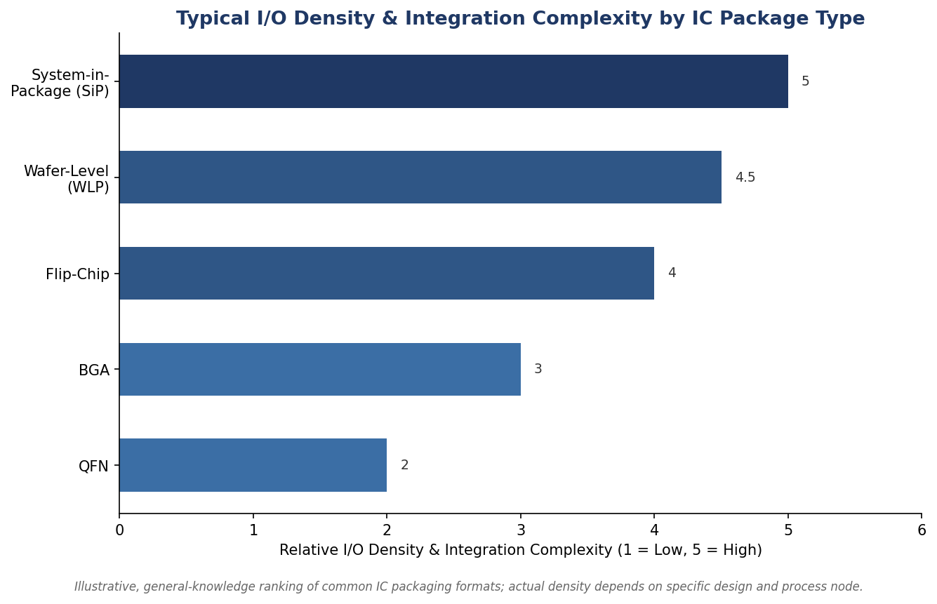

Illustrative, general-knowledge ranking of common IC packaging formats; actual density depends on the specific design and process node.
Misconception: Advanced packaging is only relevant for cutting-edge chips
Transistor-level scaling has slowed industry-wide, which has pushed much of the semiconductor industry’s remaining density and performance gains into packaging rather than the die itself. What’s now grouped under advanced packaging technologies (2.5D and 3D stacking, panel-level packaging, fan-out WLP) increasingly shows up in mainstream RF, automotive, and industrial designs, not just flagship mobile processors, because the same footprint and performance pressures exist well outside the leading edge.
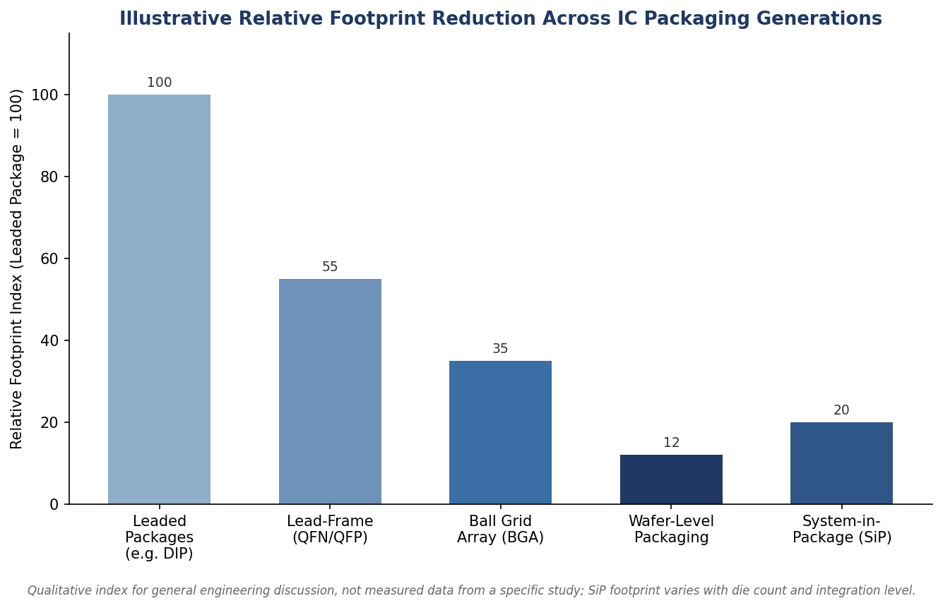
Qualitative footprint index for general engineering discussion, not measured data from a specific study; actual footprint depends on die count and integration level.
The common thread across all four of these confusions is that packaging terms describe trade-offs, not a strict hierarchy from basic to advanced. Choosing the right one depends on which constraint (footprint, I/O count, thermal performance, or integration level) actually matters for a given design.
Frequently Asked Questions
What is the difference between wafer-level packaging and traditional IC packaging?
Wafer-level packaging applies the packaging process while dies are still part of the wafer, before singulation, while traditional packaging processes each die individually after it has been cut from the wafer, generally resulting in a larger final footprint.
What is a System-in-Package (SiP)?
A System-in-Package combines multiple dies, passive components, and sometimes RF or MEMS elements into a single package, so it functions as a complete subsystem rather than a single chip.
Why is QFN packaging common in RF and power-sensitive designs?
QFN packages use a lead-frame with exposed pads on the underside instead of protruding leads, which gives a smaller footprint along with better thermal and electrical performance than older leaded package types.