Insurance Solutions
Advanced Packaging Technologies: The Architecture of Modern Electronics

Advanced packaging technologies have quietly moved from niche research to mainstream manufacturing, transforming the substrate beneath every chip into a strategically critical component of modern electronics design. As devices shrink and performance demands grow, understanding these structural form factors is no longer optional for engineers, procurement teams, or supply-chain strategists operating in 2026. This article breaks down what these formats are, why they matter, and how to evaluate the choices available today.
The global advanced semiconductor packaging market is projected to surpass $65 billion by 2027, driven by demand from AI hardware, 5G infrastructure, automotive electronics, and aerospace applications. Behind that number is a fundamental engineering problem: traditional wire-bonding and single-die approaches can no longer keep pace with modern performance requirements on their own.
Consequently, solutions providers have built integrated capabilities that span substrate fabrication, IC packaging, and assembly under one roof. This unified approach reduces lead times and simplifies qualification significantly.
What Are Advanced Packaging Technologies?
Advanced packaging refers to a family of approaches that go beyond conventional wire-bonded plastic packages to achieve higher density, lower power consumption, improved signal integrity, and a smaller physical footprint. The category includes several core variations:
-
Wafer Level Packaging (WLP): Packages chips at the wafer stage before singulation occurs.
-
Fan-Out Wafer Level Packaging (FO-WLP): Extends the redistributed I/O connections beyond the actual die footprint.
-
2.5D IC Packaging: Places multiple dies side-by-side on a shared interposer layer.
-
3D IC Packaging: Stacks dies vertically using highly dense through-silicon vias (TSVs).
-
System-in-Package (SiP): Integrates multiple heterogeneous dies into a single unified package.
-
Panel Level Packaging (PLP): Applies wafer-level concepts to large rectangular panels to achieve higher manufacturing throughput.
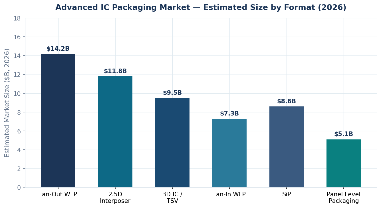
Advanced Packaging Format Market Size Index
Each format addresses a distinct set of trade-offs between cost, density, thermal management, and manufacturing yield. Therefore, understanding the economic scale of each deployment format helps engineering teams gauge industry adoption curves.
The column chart below outlines the estimated global market valuation across primary structural form factors:
Bar chart showing the 2026 estimated market size in billions for advanced packaging formats, led by Fan-Out WLP at fourteen point two billion dollars.

| Format | Key Feature | Typical Layer Count | Density | Thermal Performance | Primary Applications |
| Fan-In WLP | Die-sized package | Redistribution layer | High | Moderate |
Mobile, IoT |
| Fan-Out WLP | Extended I/O | 2–4 RDL layers | Very High | Good |
Mobile SoCs, 5G |
| 2.5D (Interposer) | Side-by-side dies | Silicon/organic interposer | Extremely High | Good |
HPC, AI accelerators |
| 3D IC / TSV | Stacked dies | TSV interconnects | Maximum | Challenging |
Memory, HPC |
| SiP | Heterogeneous integration | Multi-die substrate | High | Design-dependent |
Wearables, Defense |
| Panel Level (PLP) | Rectangular substrate | Standard litho lines | High | Good |
High-volume consumer |
Why the Shift Toward Advanced Packaging Is Accelerating
Moore’s Law scaling is no longer the primary driver of semiconductor performance. Because transistor shrinks become more expensive and physically constrained below 3nm, packaging innovation has become the next frontier. Crucial engineering drivers include:
-
Bandwidth Demands: 3D stacking of DRAM on logic delivers orders-of-magnitude more bandwidth than traditional DRAM modules.
-
Power Efficiency: Shorter interconnects in 3D and 2.5D packages reduce parasitic capacitance and switching losses.
-
Heterogeneous Integration: Combining logic, analog, RF, and memory chiplets in a single SiP allows best-of-breed process nodes for each function.
-
Form Factor Constraints: Wearables, aerospace avionics, and medical implants simply cannot accommodate conventional multi-chip layouts.
Furthermore, the defense and aerospace sectors have been early adopters where ruggedization and space constraints are non-negotiable. Production of complex defense electronics depends on substrates capable of reliable operation under extreme vibration, temperature cycling, and RF environments. For this reason, selecting a partner proficient in semiconductor packaging solutions ensures maximum hardware survivability in harsh theater deployments.
Organic Substrates vs. Silicon Interposers: The Foundation Matters
The substrate in advanced packaging defines the electrical performance and manufacturability ceiling of the entire package. The two dominant substrate classes are organic substrates and silicon interposers.
Organic substrates are lower cost and compatible with standard PCB manufacturing lines. In contrast, silicon interposers deliver the highest density and performance but carry longer lead times. Organic substrate manufacturers capable of modified semi-additive process (MSAP) patterning occupy a critical position in the supply chain. This occurs because MSAP enables the fine line/space features required for advanced redistribution layers without the extreme cost floor of silicon.
Selecting the Right Advanced Packaging Approach
No single packaging format is universally superior. Consequently, teams should establish a structured selection framework before finalizing component designs.
First, look at manufacturing volume, since fan-out and PLP offer clear cost advantages at scale. Second, assess the thermal envelope because 3D stacking concentrates heat and requires careful thermal co-design. Third, evaluate time-to-market constraints, as organic substrate approaches typically have shorter qualification cycles than silicon interposer flows. Finally, manage supply-chain risk by ensuring that single-source substrates do not introduce critical configuration bottlenecks.
Conclusion
Advanced packaging formats have moved from research labs to volume production lines. The choice of packaging format has a direct impact on power, performance, area, cost, and supply-chain resilience. As demand from AI, defense, and communications continues to accelerate, evaluating suppliers and technologies against these parameters becomes the defining task of modern hardware strategy. To implement a qualified production run, engineers frequently combine multi-layer routing paths with specialized ic packaging services under a single manufacturing umbrella.